0
\$\begingroup\$

An 8 Kbyte ROM with an active low Chip Select input (CS') is to be used in an 8085 microprocessor based system. The ROM should occupy the address range 1000 H to 2FFFH. The address lines are designed as A15 to A0 , where A15 is the most significant address bit. Which one of the following logic expressions will generate the correct CS signal for this ROM?

(A) A15 + A14 + (A13.A12+A13'.A12')

(B) A15.A14.(A13 + A12)

(C) A15' + A14'.(A13.A12' + A13'.A12)

(D) A15' + A14'+ A13.A12

(Question credit: EC-Gate 2016 SET-2)

I am trying to learn digital circuits on my own. Above is a question I am unable to solve.

According to me, the aim is to choose an option which would make the chip select signal to be 0. So both option A and B should be correct, but that is not the case. Moreover, A12 is address line for the ROM so how can we use it for CS signal.

Edit: Thanks @AJN and @Brian Drummond. I understood why option A is correct and not B but I have one more confusion, according to what I know some of the address lines coming out of the 8085 are used as address lines for the memory (ROM in this case) and others (the higher order address lines) are used as the chip select signal. My question is that when A12 is used as address lines for the ROM then can we use it for CS signal also. According to me A15, A14 and A13 should go to chip select signal and others should go to the address lines.

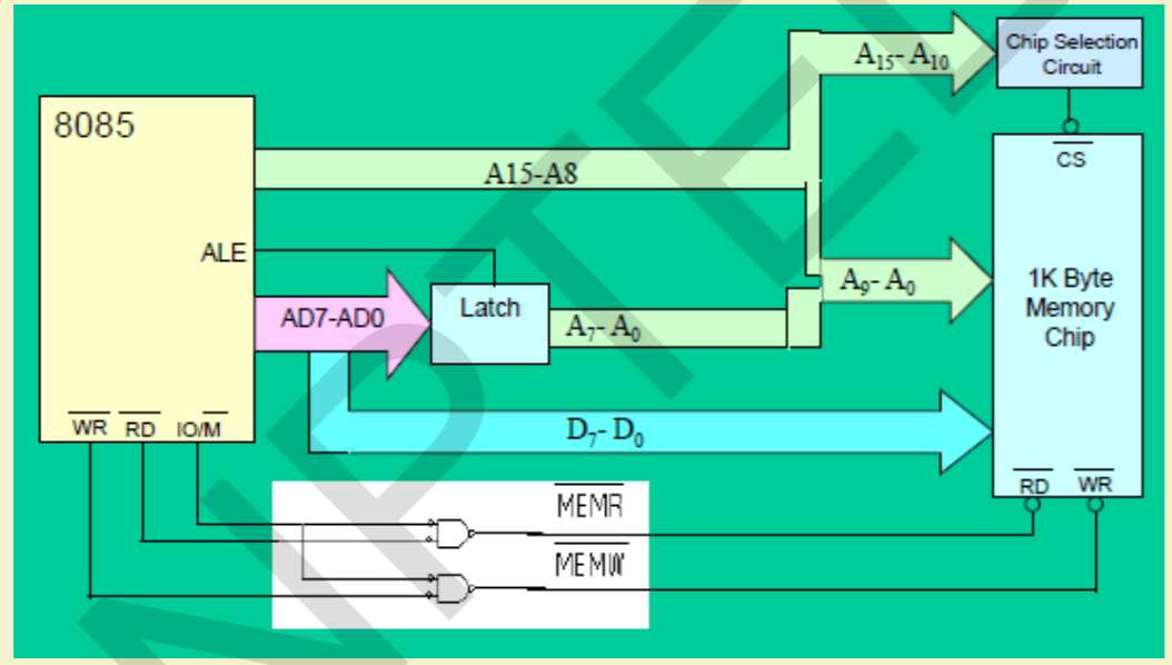
The Overall Picture

\$\endgroup\$
8
  • \$\begingroup\$ Well which addresses do the equations decode to, and which one matches the required address? \$\endgroup\$
    – Justme
    Commented Sep 27, 2020 at 12:16
  • \$\begingroup\$ Options A, B, C, D are equations for the CS signal. Which one of the following logic expression will generate correct CS signal for the ROM. \$\endgroup\$ Commented Sep 27, 2020 at 12:18
  • 1
    \$\begingroup\$ Demanding the correct answer without knowing why it is the correct answer will not help you learn anything. \$\endgroup\$
    – Justme
    Commented Sep 27, 2020 at 12:23
  • 2
    \$\begingroup\$ Write a truth table for A15-A12 and see which satisfies it. There is a nasty practical issue of the ROM not being aligned, but that's not an issue for /CS generation. \$\endgroup\$ Commented Sep 27, 2020 at 12:42
  • 3
    \$\begingroup\$ Making the CS = 0 for the correct addresses is only half the problem. You must also ensure it is 1 outside the correct address range. Review the choices with that in mind. \$\endgroup\$
    – user16324
    Commented Sep 27, 2020 at 13:01

2 Answers 2

2
\$\begingroup\$

Image the address is 0x4000. Option (B) gives 0.1.(0+0)=0. The chip is selected even though the address is outside the range. You need to check not just if the options will give 0 for addresses in-range, but 1 for addresses outside the range.

Moreover, A12 is address line for the ROM so how can we use it for CS signal.

I don't understand fully, but the line coming out of the 8085 can be split into two traces, and connected to both the ROM and the CS generating circuit.

\$\endgroup\$
4
  • \$\begingroup\$ What is it that you did not understood. What I meant is that some of the address lines coming out of the 8085 are used as address lines for the memory (ROM in this case) and others (the higher order address lines) are used as the chip select signal. My question is that when A12 is used as address lines for the ROM then can we use it for CS signal also. \$\endgroup\$ Commented Sep 27, 2020 at 13:03
  • 1
    \$\begingroup\$ That will happen any time the memory is not sitting a "natural" position in the address space -- in other words, the assigned address range has boundaries that are not multiples of the memory's size. When that happens, you need to use one or more of the address lines in both places. \$\endgroup\$
    – Dave Tweed
    Commented Sep 27, 2020 at 13:19
  • 1
    \$\begingroup\$ Because you need A12 for both things. A12 needs to be used for Chip Select to get the correct address, without it, Chip Select will be wrong. A12 needs to be used also as ROM memory address to select which 4k half of the 8k chip is used. \$\endgroup\$
    – Justme
    Commented Sep 27, 2020 at 13:21
  • 1
    \$\begingroup\$ "My question is that when A12 is used as address lines for the ROM then can we use it for CS signal also". Like mentioned in the answer, "the line coming out of the 8085 can be split into two traces". So, yes, it can be used for two purposes. \$\endgroup\$
    – AJN
    Commented Sep 27, 2020 at 15:32
0
\$\begingroup\$

The memory range is given as 1000H to 2FFFH. This chip will be selected when A15 = A14 = 0 and A13 and A12 are not the same.

All these four signals are ORed together to produce low signal to chip select i.e. A15, A14, A13, A12 will be 0001 or 0010.

So A15 + A14 + (A13'.A12' + A13.A12) may produce the required logic.

\$\endgroup\$

Your Answer

By clicking “Post Your Answer”, you agree to our terms of service and acknowledge you have read our privacy policy.

Not the answer you're looking for? Browse other questions tagged or ask your own question.