1
\$\begingroup\$

My final project for my electronics class is to design a three stage transistor amplifier. The final project
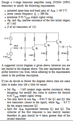
I'm not asking for answers, or for someone to do this project for me. I need help starting the project and a general set of steps that I can follow for deriving an expression for V_out.

When I draw a miller equivalent circuit for this amp, V_out is across that 50k resistor at the emitter. Previous circuits in the class have had V_out taken from the collector, which made it easy to derive an expression for V_out after multiple voltage divisions.

Additionally, is there any way that I can calculate the resistor values? Or should I load the circuit up in a Spice program and guess resistors until I get an acceptable A_mb and f_L?

My study group is super lost on this :( We haven't gotten any circuits this complex and with so many missing values during the semester.

\$\endgroup\$
9
  • 2
    \$\begingroup\$ Well why don't you start off by taking each of the requirements and giving us your thoughts on how you will achieve them and what component choices are dictated. For example the question is asking you to split the gain between the Q1 and Q2 stage-so what is the gain of the Q1 stage in this case and what is the value of the collector resistor that will achieve this gain? Which parts of the circuit will have a specific frequency response-what values of the components will give you the desired corner frequency? \$\endgroup\$
    – mhaselup
    Commented Nov 24, 2020 at 4:00
  • \$\begingroup\$ Since your requirements do not make you use specifically that circuit, I would rather use a three stage amplifier AC coupled with capacitors, that way you can set the bias point exactly where you want it without much complications, you can also bias each stage at the middle of the AC and DC load line so you get maximum symetrical output swing. \$\endgroup\$
    – S.s.
    Commented Nov 24, 2020 at 4:17
  • 2
    \$\begingroup\$ One question comes to mind. The schematic, which appears to be part of the specification, shows an input signal of \$1\:\text{mV}_\text{PK}\$. But the specification also says that you must exhibit an output minimum of \$250\:\text{mV}_\text{PK}\$. While it also says that \$A_v\ge 50\$. It seems to me that you have to achieve at least \$A_v\ge 250\$, at a glance. So, is there a conflict? Or am I missing something? For example, are you allowed in increase the input signal? It does not seem so from my reading. But perhaps it can be? \$\endgroup\$
    – jonk
    Commented Nov 24, 2020 at 5:39
  • \$\begingroup\$ @jonk 250 is greater than 50! \$\endgroup\$ Commented Nov 24, 2020 at 13:59
  • \$\begingroup\$ @StainlessSteelRat It is. But the point is that the one spec seems unnecessary, then. Perhaps giving question to the whole thing. If they came from a marketing stooge, I'd just move on. But if from an engineer, I'd question their sanity. \$\endgroup\$
    – jonk
    Commented Nov 24, 2020 at 14:02

2 Answers 2

1
\$\begingroup\$

For starters, to proceed with low distortion in mind, bias that first transistor to have the Vout at VDD/2.

Then bias the 2nd transistor to have Vout at 3/4 * VDD.

What does this allow?

What gains are achievable?

Then, if necessary, adjust your bias points.

======================================================

The maximum gain you can achieve with ONE bipolar transistor (so we are focusing on just that first transistor, for now) is VDD/0.026 volts.

In this case, with 15 volts, the maximum gain is 15/0.026 = 15 * 39 ~~ 600.

This formula assumes NO EMITTER RESISTOR. There is a 1Kohm in the emitter.

Working with that, let us get the gain of 50 in that first transistor.

Ignoring (initially) the 'reac' of that transistor (the 1/gm), for a gain of 50 we need 50 = Rcollector / 1Kohm, which is ignoring the loading effect of the 2nd stage.

This suggests the Rcollector be 50Kohm.

Now adjust the biasing network (on base of first transistor) to place Vce at about 7.5 volts.

Now compute the actual gain achieved, given a finite 1/gm of the first transistor.

What will the collector current be? 7.5 volts / 50,000 ohms

And 50,000 ohms is also 20 uAmp/volt, so Ic = 20 * 7.5 = 150 microAmps.

Across that 1Kohm in the emitter, Vemitter = 0.150 volts.

Now design the base_biasing network, including the base current demand.

And compute the achieved gain: 50,000 ohms / (1K + 1/gm_Q1)

Now you need to consider what to do with Q2.

By the way, notice the gain of that first stage will be lower than 50x. Why?

  • the small_signal resistance of the transistor's diode (BE junction) gets added to the 1Kohm Remitter

  • the loading effect of Rin of the 2nd transistor, which will be beta * that Re, thus 150 * 1Kohm = 150,000 ohm

\$\endgroup\$
-1
\$\begingroup\$

"Previous circuits in the class have had V_out taken from the collector, which made it easy to derive an expression for V_out after multiple voltage divisions."

The last stage is an emitter follower (also known as a common collector amplifier). The emitter voltage closely follows the base voltage less one \$V_{BE}\$. The base voltage for the last stage is clearly \$V_{OUT}\$ of the previous stage.

"Additionally, is there any way that I can calculate the resistor values? Or should I load the circuit up in a Spice program and guess resistors until I get an acceptable A_mb and f_L?"

The voltage gain of a common emitter amplifier can be calculated from \$\frac{R_L}{R_E + R_e}\$ where \$R_e\$ is the intrinsic emitter resistance. If \$R_E\$ is large, \$R_e\$ can be ignored. Otherwise, \$R_e\$ can be calculated from \$I_E\$.

\$\endgroup\$

Your Answer

By clicking “Post Your Answer”, you agree to our terms of service and acknowledge you have read our privacy policy.

Not the answer you're looking for? Browse other questions tagged or ask your own question.