1
\$\begingroup\$

I'm looking for the circuit to automatically switch the load (< 0.5 A) between the main power source (USB) and back-up (battery) without a specialized IC and without the functionality of charging the battery.

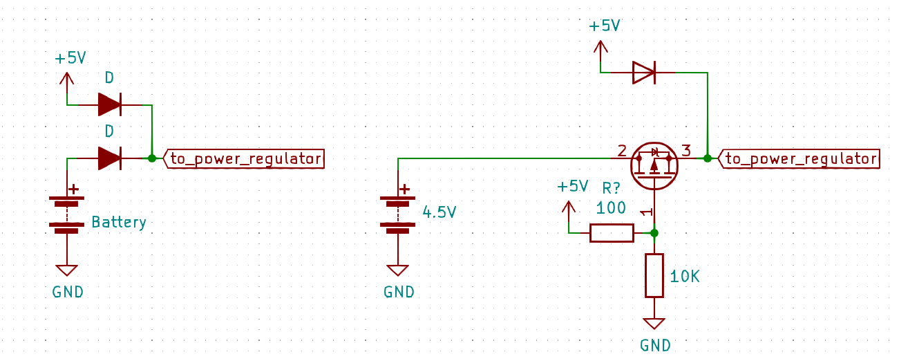
I found two options:

  • with 2 diodes
  • diode from the main source and switchable P-MOSFET from the battery enter image description here

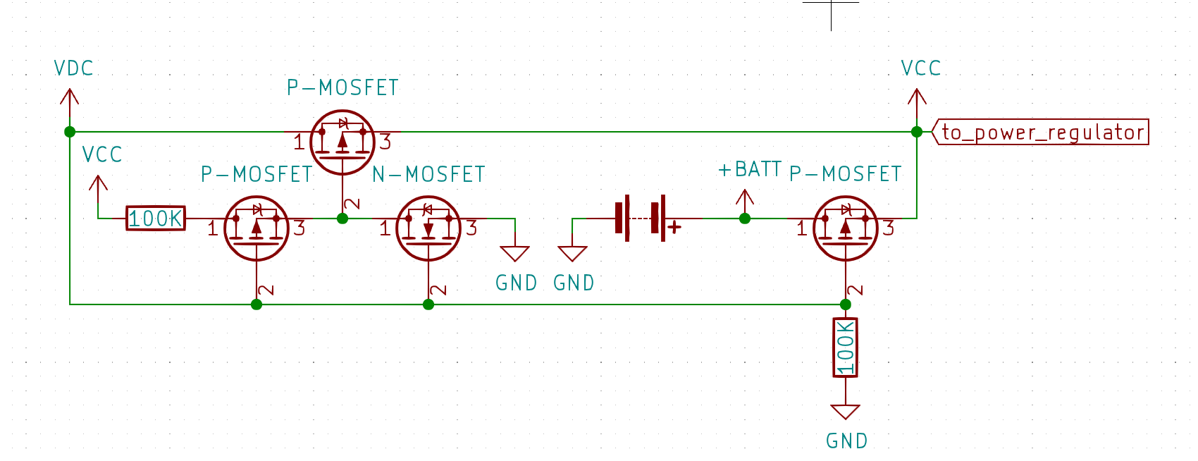
I wonder if a similar solution can be implemented with MOSFETs only and came up with the following circuit:

enter image description here

Where VDC is the external power source, +BATT is voltage from battery, and VCC is the output voltage (automatically switched).

To my understanding (I'm not an EE) this should work as follows:

  • if VDC is connected:
    • the top P-MOSFET connects the VDC to VCC since the lower N-MOSFET shortens the gate of top P-MOSFET to GND and opens it
    • other P-MOSFETs are closed.
    • VDC = VCC
  • if VDC is not connected:
    • the VDC is pulled to GND, it opens the left bottom P-MOSFET, which pulls the top P-MOSFET to the VCC and closes it to prevent the back-flow from VCC to VDD
    • P-MOSFET connected to battery is open and connects the battery to load
    • VCC = +BATT

My questionas are:

  • Is it going to work? In case if VDC is USB and +BATT is 3xAAA batteries? Or if +BATT is a LiIon battery?
  • Is this solution any better in terms of saving energy than option with 2 diodes and/ one diode and mosfet? Are the voltage drops lower in such schematic?
  • Are there any other problems in this schematics except the hustle to find P-mosfers which can be open from small batteries voltage?
  • This circuit is going to work only if VDC > (+BATT + body voltage drop on right bottom P-MOSFET)?
\$\endgroup\$
1
  • \$\begingroup\$ As I understand, in given circuits the P-FETs function as reverse polarity protection, and because of that the drain and source should be reversed (interchanged) intentionally according to this \$\endgroup\$ Commented Nov 30, 2020 at 12:14

1 Answer 1

0
\$\begingroup\$

In principle this circuit should work, however here are two suggestions:

  • Remove the \$100k\Omega\$ resistor between VCC and the leftmost PFET. This resistor is slowing down the gate charging of the upper PFET during the VDC to BATTERY switchover. Meaning that, for a couple of miliseconds the battery might discharge into VDC if the latter \$VDC< V_{BAT} - V_{BD}\$.

  • Add some capacitance at the node VCC in order to account for voltage dips during the switchover.

Update#1

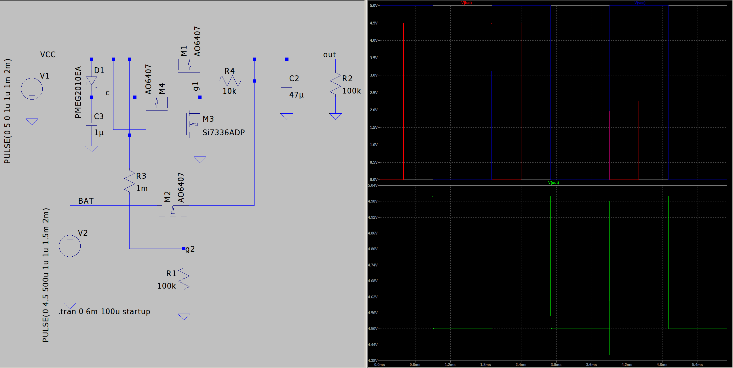
The following simulation introduces a buffering capacitor \$C_1\$ which speeds up the gate capacitance charging of the upper PFET. Essentially the capacitor \$C_1\$ is charged when the VCC is active, and once the latter is disconnected, the capacitor discharges into the gate capacitance of the upper PFET.

circuit_1

\$\endgroup\$
3
  • \$\begingroup\$ I did doubt if that resistor was necessary, and my concern is if without it there could be potentially a situation when VCC is shortened to GND. Is it possible? Regarding the capacitor: there will be a voltage regulator downstream with the incoming capacitor. I'll count for that. \$\endgroup\$ Commented Nov 28, 2020 at 15:29
  • 1
    \$\begingroup\$ If you also want to cover this malfunction, you could keep the resistor but also add some additional voltage buffering for charging the gate capacitance of the upper mosfet. I will update my answer with some small simulation. \$\endgroup\$
    – vtolentino
    Commented Nov 28, 2020 at 17:18
  • 1
    \$\begingroup\$ Thank you! Probably, I also need to test this circuit in hardware. \$\endgroup\$ Commented Nov 30, 2020 at 12:09

Your Answer

By clicking “Post Your Answer”, you agree to our terms of service and acknowledge you have read our privacy policy.

Not the answer you're looking for? Browse other questions tagged or ask your own question.