1
\$\begingroup\$

enter image description here

In order to stay in the saturation, the voltage between collector and emitter has to be exactly equal to Vce in the char above, is that right?

But when the transistor is working at Vce and 0 < Ib < (Ic/beta), meaning Ic is not at the maximum capability for the transistor. The voltage drop between collector and emitter is a fixed value for the transistor made of certain material (0.7V for silicon and 0.2V for germanium). Is that right?

And, Rc, the resistor in serial with collector takes the remaining of the voltage from power supply. E.g., 5V power supply Vce is 0.7V, as long as the transistor is open. And, the voltage left for resistors in serial with collector is 5V - 0.7V = 4.3V. Is that right?

So, the value for Rc to limit the current Ic from its maximum, say 0.6A, would be 4.3V / 0.6A = 7.17 Ohm?

When using voltage divider(two resistors in series) to control the Ub, voltage at base, making Ub higher than the 0.7V voltage drop required for Ube to open the transistor, why could the Ub be higher than 0.7v? I thought Ub would always stay at 0.7V for silicon knots and 0.2V for germanium knots.

As I'm still waiting for my NPN transistors to arrive to do experiment, my breadboard experiment with PNP transistor BC557 B shows, when Ub is lower than Ue, which is required to open the transistor, it seems Ub is decided by Uc minus the voltage drop between c and b, instead of the voltage divider for base pin.

Thanks!

\$\endgroup\$
4
  • 1
    \$\begingroup\$ Don't you want the BJT to stay in the active region? (I've a hunch, reading through your questions, that you have many thoughts that need to be tossed overboard and then new ones acquired.) \$\endgroup\$
    – jonk
    Commented Dec 1, 2020 at 1:18
  • \$\begingroup\$ "The voltage drop between collector and emitter is a fixed value for the transistor made of certain material (0.7V for silicon and 0.2V for germanium)" No, it is not fixed and those are the (conventional) values for Vbe. Also, that diagram is misleading to say the least. The operating point of the transistor is constrained to be on the intersection of the load line with one of the output curves. It will not fall in the shaded areas. \$\endgroup\$ Commented Dec 1, 2020 at 1:22
  • 2
    \$\begingroup\$ Voting to close on the grounds that this needs more clarity. Specifically, you need to ask just one question at a time -- you're asking a whole bunch of unrelated questions, and your later questions are based on erroneous assumptions about the answers to the earlier questions. Why don't you edit your question to stop at the first question mark. We'll answer that, then you can post the next one, we'll work through that, etc. \$\endgroup\$
    – TimWescott
    Commented Dec 1, 2020 at 1:42
  • \$\begingroup\$ Base to emitter voltage depends on base current and temperature of the transistor. Hotter temps = lower voltage for same current (this is linear). Higher current = higher voltage, but it is non-linear. Doubling the base current will only make the base voltage slightly higher. \$\endgroup\$
    – user57037
    Commented Dec 1, 2020 at 2:01

2 Answers 2

1
\$\begingroup\$

How to analyze saturated switch circuits.

First, figure out how much collector current you want when the switch is on. Assume that the voltage from collector to emitter is Vce(sat) from the datasheet. It could be something like 0.2V for some transistors or 1V for others, depending on how much current and type of transistor.

Second, divide the desired collector current by 10 or 20. This number, 10 or 20 is called the forced beta (beta(forced)).

Third, arrange to drive the base with Ic/Beta(forced).

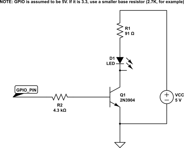
Full example. I have an LED that I want to drive with 20mA. VCC is 5V. The datasheet for the LED says Vf is 3V at If = 20mA. So I want Ic to be 20mA.

Vce(sat) for my 2N3904 is 0.2V at 20mA. So after I subtract Vce(sat) and Vf from VCC I have 1.8V left to drop across my resistor. So the resistor value needs to be 1.8V/20mA = 90 Ohms (pick the nearest value, e.g., 91 Ohms).

I am driving the base of the transistor with an IO pin from my microprocessor (VCC = 5V). I am going to use a forced beta of 20. So I want my base current to be 1mA. The base is going to be at around 0.7V with 1mA going through it. So the base resistor needs to drop 4.3V with current of 1mA. This means the base resistor needs to be 4.3k, which is a standard value.

This is how you handle a saturated switch. From the perspective of cause and effect, the way it works is when you drive the base hard, it pushes the transistor into saturation. To achieve saturation, you always want to supply an excess of current to the base to push Vce down lower. It is the base current that causes Vce to drop. By supplying excess current to the base you are forcing the transistor to operate in low beta. That is why they call it forced beta.

schematic

simulate this circuit – Schematic created using CircuitLab

\$\endgroup\$
1
  • \$\begingroup\$ The definition of saturation is that both transistor junctions are under forward bias. So base to emitter must be forward biased, and base to collector must also be forward biased. \$\endgroup\$
    – user57037
    Commented Dec 1, 2020 at 2:07
1
\$\begingroup\$

In order to stay in the saturation, the voltage between collector and emitter has to be exactly equal to Vce in the char above, is that right?

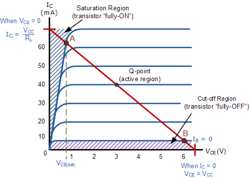
In a bipolar transistor 'saturation' means that VCE is as low as it can get at that Collector current, effectively changing from a controlled current source to a resistor. In this region IC is no longer proportional to IB, ie. the transistor is 'saturated' with Base current and cannot turn on any harder.

But when the transistor is working at Vce and 0 < Ib < (Ic/beta), meaning Ic is not at the maximum capability for the transistor. The voltage drop between collector and emitter is a fixed value for the transistor made of certain material (0.7V for silicon and 0.2V for germanium). Is that right?

You seem to be a bit confused here. VBE is often considered to be a fixed value of 0.7 V for silicon. When not in saturation VCE slides up and down (along the red 'load line' in the graph) as IC varies, due to varying voltage drop across the load.

The load line in that graph is just an example for particular load resistance (in this case 100 Ω), and point 'A' is VCE(sat) for that load only. If the load resistance was higher the line would intercept the Y axis lower down, and VCE(sat) would be lower.

And, Rc, the resistor in serial with collector takes the remaining of the voltage from power supply. E.g., 5V power supply Vce is 0.7V, as long as the transistor is open. And, the voltage left for resistors in serial with collector is 5V - 0.7V = 4.3V. Is that right?

Yes.

So, the value for Rc to limit the current Ic from its maximum, say 0.6A, would be 4.3V / 0.6A = 7.17 Ohm?

Yes, but only if VCE(sat) is 0.7 V at IC = 0.6 A. Depending on the transistor it could be higher or lower. In your graph VCE(sat) is ~0.7 V at 60 mA, so at 600 mA it would be much higher (~7 V, assuming linear extrapolation).

When using voltage divider(two resistors in series) to control the Ub, voltage at base, making Ub higher than the 0.7V voltage drop required for Ube to open the transistor, why could the Ub be higher than 0.7v? I thought Ub would always stay at 0.7V for silicon... and 0.2V for germanium

The 0.7 V and 0.2 V are only approximations used for calculating bias resistors etc., the actual voltage increases as Base current increases.

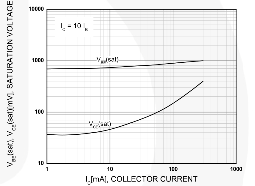
Here is a graph of VBE(sat) (and VCE(sat)) vs IC for BC547-BC550:-
enter image description here

At a Base current of 100 μA (IC = 1 mA) VBE is indeed 0.7 V, but at higher Base current it increases (to ~1 V at 30 mA). In linear operation IB is usually less than 1 mA, so 0.7 V is close enough for most calculations.

Note that this transistor's absolute maximum DC Collector current rating is 100 mA, at which point VCE(sat) is typically ~150 mV. if running from a 5 V supply the minimum load resistor permitted to limit Collector current to 100 mA would be (5-0.15)/0.1 = 48.5 Ω. In practice a higher resistance would be chosen to reduce Collector current and improve reliability.

\$\endgroup\$

Your Answer

By clicking “Post Your Answer”, you agree to our terms of service and acknowledge you have read our privacy policy.

Not the answer you're looking for? Browse other questions tagged or ask your own question.