1
\$\begingroup\$

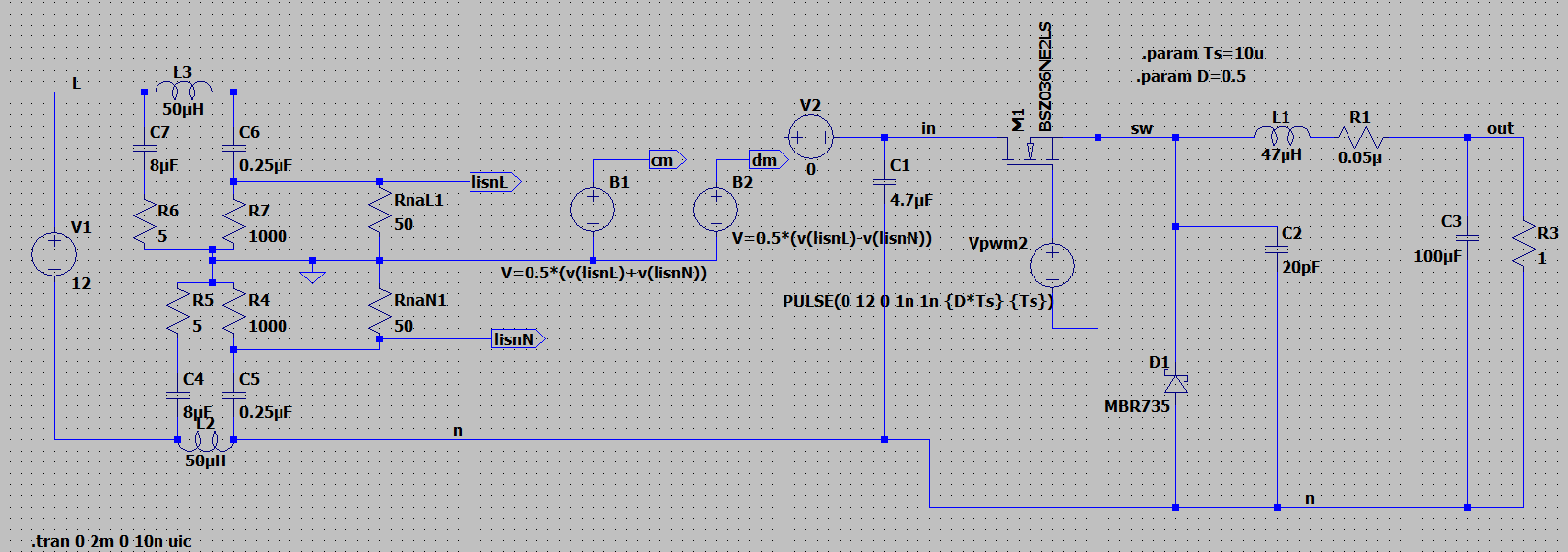
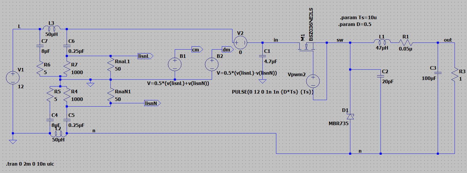
I am trying to do an elementary EMI analysis on my Buck converter circuit by modelling the LISN circuit. I am using LTSpice for this. The buck converter works when I simply simulate this circuit alone:-

buck

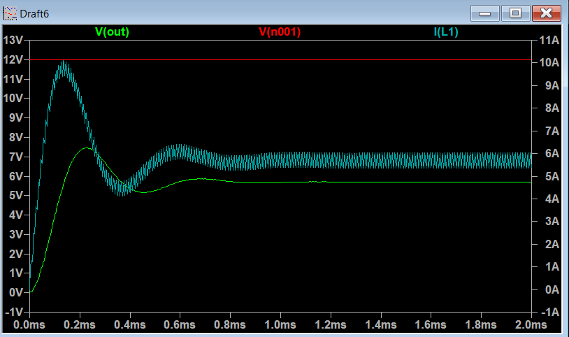
Here is the waveforms for this circuit:-

waveforms

But when I try to add the LISN circuit with this I am getting wrong output voltages and thus wrong everything else. What am I doing wrong? I suspect it is something to do with the net labels but I cannot get it right.

lisn

Waveforms for this:-

waveform2

EDIT 1:- I made the suggested changes in the circuit and this is the waveforms I get:- Vout new circuit switching node

Is the Vpwm1 correct? I am getting a wrong switching waveform.

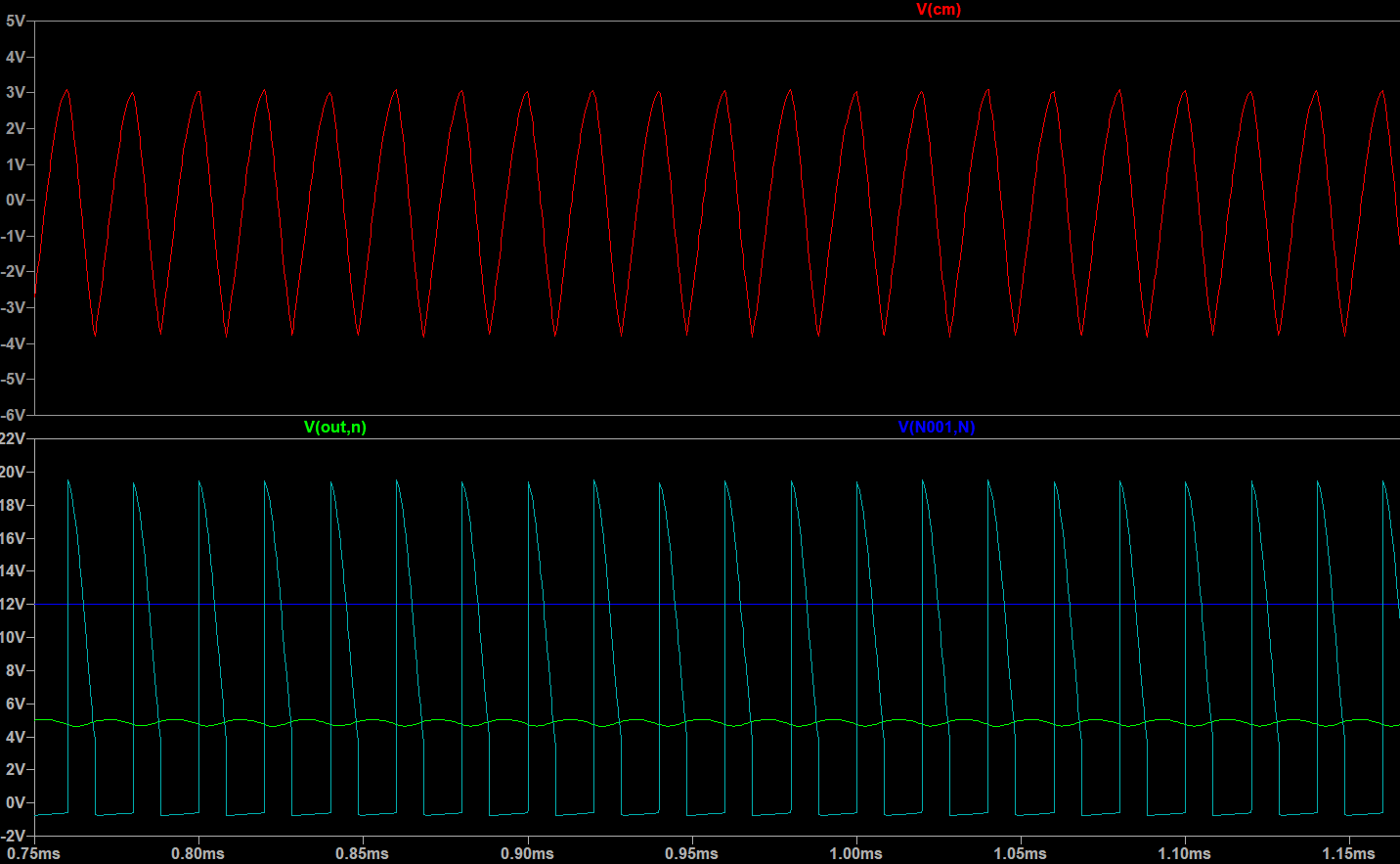
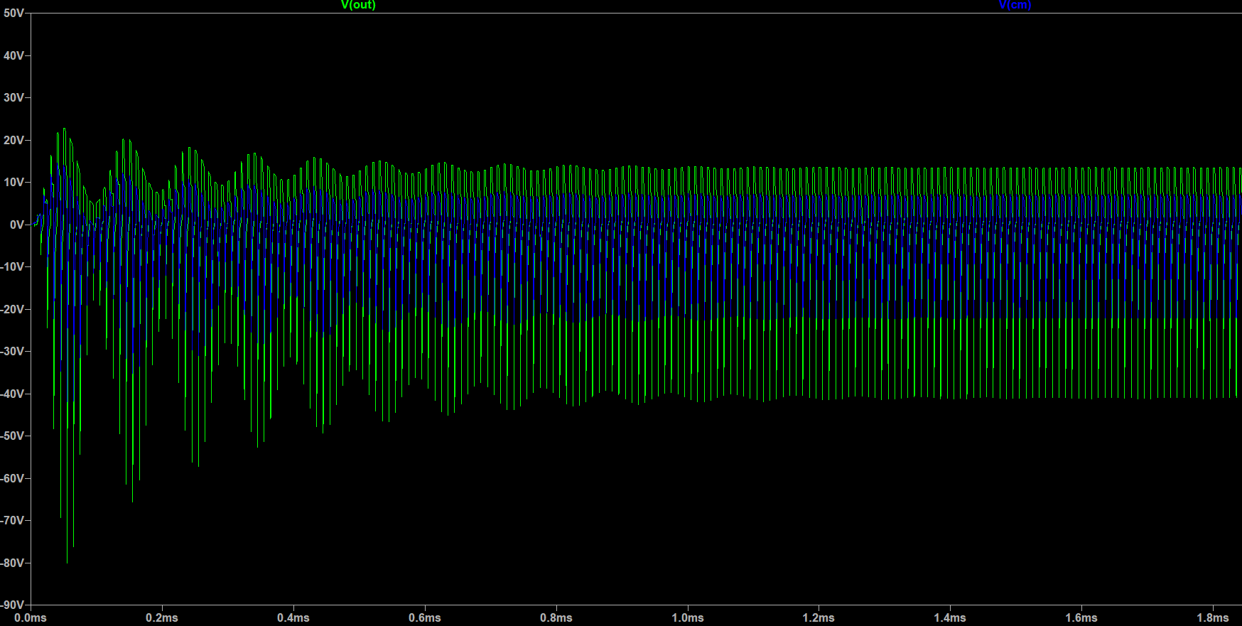
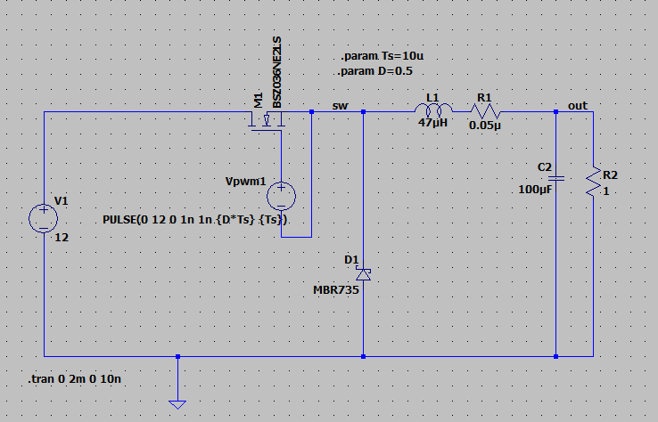
EDIT:2 After several comments, I have realized the problem lies with the LISN circuit, but I don't know how to set the inductors and capacitors of this module. As per Bruce Abbott's suggestion I lowered it to 5uH but still not getting the right common mode and differential mode voltages, although the output voltage is correct. This is a buck converter (12 V to 5 V @200 kHz):- buck Here is the waveforms:- waveforms How do I fix the C6 value and the LISN L & C values? [This is just for simulation on LTSpice, the real PCB is being simulated on ANSYS SIwave)

\$\endgroup\$
11
  • \$\begingroup\$ It looks like whoever posted the previous answer deleted it. It said the EMC is not something you simulate with a SPICE simulator, but rather with a FEMM or similar. There was also a comment pointing towards a possible similar question. \$\endgroup\$ Commented Dec 3, 2020 at 20:22
  • \$\begingroup\$ @aconcernedcitizen Yes I'm simulating the actual PCB using ANSYS SIwave,but I thought it better to understand the basics properly using LTSpice. Thank you for the link. \$\endgroup\$
    – SM32
    Commented Dec 4, 2020 at 4:18
  • \$\begingroup\$ R1 seems unrealistically low to me. Perhaps it should be 0.05 ohms rather than 0.05 micro-ohms? \$\endgroup\$ Commented Dec 4, 2020 at 5:36
  • \$\begingroup\$ In what way is the switching waveform 'wrong'? \$\endgroup\$ Commented Dec 4, 2020 at 8:03
  • \$\begingroup\$ @BruceAbbott The "sw" node voltage waveform should have been like a square wave, like a PWM voltage waveform....but it isn't here \$\endgroup\$
    – SM32
    Commented Dec 4, 2020 at 10:01

1 Answer 1

1
\$\begingroup\$

When drawing the LISN into your schematic you have to decide where you are placing your GND symbol.

I notice that you have a GND symbol at the bottom of V1 and also in the center of the LISN. That's not correct because C4 and R5 are connected to GND at both ends.

Also remember that (as things are drawn right now) the reference point for your "out" node is node "n" rather than ground. So to get the supply output voltage you must measure V(out) - V(n) rather than just V(out) relative to ground.

\$\endgroup\$
1
  • \$\begingroup\$ Thank you for pointing out that GND mistake.I still don't get even the correct switching waveform, although the output seems to be a bit closer to the actual waveform,but yes wrong.Kindly see the edit. \$\endgroup\$
    – SM32
    Commented Dec 4, 2020 at 4:42

Your Answer

By clicking “Post Your Answer”, you agree to our terms of service and acknowledge you have read our privacy policy.

Not the answer you're looking for? Browse other questions tagged or ask your own question.