Is there a standard for the sizes of PCB traces?
That is are some 25 mil and others 10 mil or is can you choose your own?
I plan to run 400mA through some thicker traces, but less than 30mA for all other traces. About what size would I need?
Is there a standard for the sizes of PCB traces?
That is are some 25 mil and others 10 mil or is can you choose your own?
I plan to run 400mA through some thicker traces, but less than 30mA for all other traces. About what size would I need?
Your traces can be any size you want as long as you stay within the minimum feature size and spacing that your PCB fab supports for your particular price point.
These will cover basic needs, the trace width one is a best fit calculation to the chart Engen posted:
Neither of those cover controlled impedance calculations, if you need those look elsewhere.
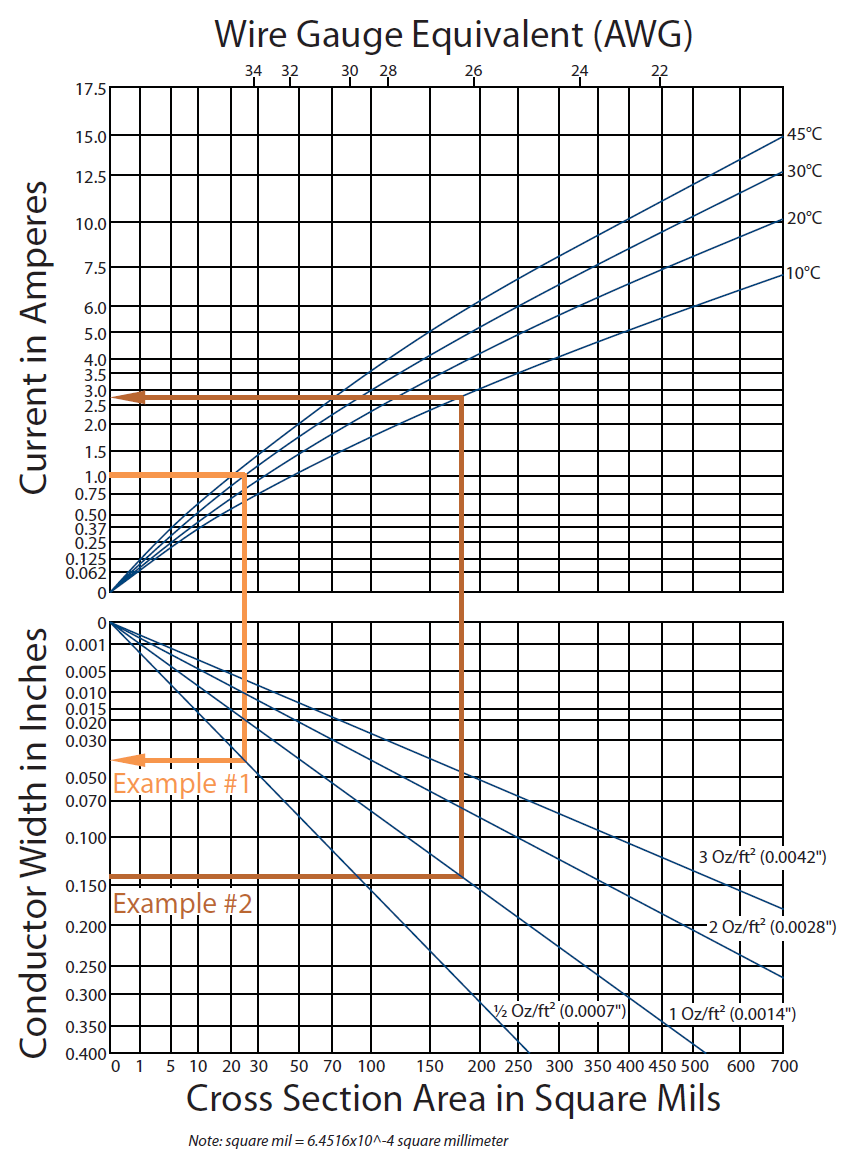
You can use this nomograph to determine the width according with current:

Using the nomograph
Locate the width of the conductor on the left side of the bottom chart.
Move right horizontally, until you intersect the line of the appropriate conductor thickness. Move down vertically to the bottom of the chart to determine the cross-sectional area of the conductor.
Move up vertically, until you intersect the line of the appropriate allowable temperature rise. This is the increase in temperature of the current-carrying conductor. Conductor temperature should not exceed 105°C. For example, if the ambient temperature might reach 80°C, the temperature rise above ambient of the conductor should be less than 25°C (105°C - 80°C). In this case use the 20°C curve.
Move left horizontally, to the left side if the chart to determine the maximum allowable current.
Reverse the order of these steps to calculate required conductor width for a given current.
More informations at this site: http://www.minco.com/products/flex.aspx?id=1124
This graph is from IPC, but I cannot find it there.
PCB makers sometimes produce swag that has this kind of thing on it, because it's common to want to get a feel for PCB traces that are out of one's comfort zone.
Here's a photo of one such trade-show give-away, with a dime for scale (as well as the ruler scales). Trace/space widths are in inches.

If you are making your own boards, then you want traces as large as you can get by with -- perhaps 15 mils (0.015") for signal traces, and 30 mils for power. Note: with traces that large, you will typically have to narrow the traces down a bit before connecting to IC's pins with fine pitch pads.
If you are having a board house make your boards, then you can use smaller traces for signal traces, say 8 or 10 mils if you have room. Most PCB fabricators that do fast and inexpensive boards have a minimum trace width of 5 or 6 mils, but if you can go a little larger, the better. (For military and other high-tech boards, they can now go as small as 2.5 mils or even smaller.)
For power traces, then I agree with other posts that you should use a trace width calculator like this one. I generally end up using 20 or 25 mil traces for power rails. But the calculator will give you ridiculously small trace widths for signal traces that might carry only a few milliamps.
Note that in addition to trace widths, you will also want to space your traces apart, typically by the same distance as the trace width.
You can enter these rules such as minimum trace widths and minimum distances between traces, between traces and vias etc. into Design Rule Checks in programs like Eagle layout software, and when you run a DRC the program will point out violations.
Charts
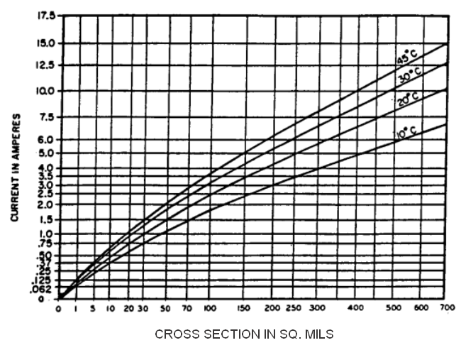
IPC standard 2221 "Generic Standard on Printed Board Design" (pdf, IPC web-site paid) (page 41) provides the following relationships between current carrying capacity and copper trace width:
 Figure 1: Cross section area to current. External layer.
Notes for the figure (also applicable for the Figure 2):
1) Temperature stands for temperature of the trace relative to ambient. That is, if, for instance, ambient temperature is 80C, 20C stands for 100C temperature of the trace.
2) The curves include a nominal 10% derating (on a current basis) to allow for normal variations in etching techniques, copper thickness, conductor width estimates and cross-sectional area.
3) Additional derating of 15% (current-wise) is suggested under the following conditions:
. a) for panel thickness of 0.8 mm or less,
. b) for conductor thickness of 108 um or thicker.
 Figure 2: Cross section area to current. Internal layer.
 Figure 3: Cross section area to trace width.
What is 1 oz copper?
The measure for the copper thickness on a printed circuit board. It's the resulting thickness (height) when 1 oz of copper is pressed flat and spread evenly over a one square foot area. It corresponds to copper thickness of 1.37 mils (34.79 um).
Explaining the relationship between cross section area and trace width (Figure 3)
1) Every curve corresponds to a particular copper thickness (trace height).
2) Area (horizontal axis) is calculated as product of trace width and thickness.
Below is a Matlab script with a calculation example. It shows that for 1 oz copper trace with the area of 9 sq. mils, trace width is 6.6 mils:
thickness=1.37E-3;%inches
area=9*(1E-3)^2;%square inches
width=(area/thickness)*(1/1E-3) %in mils
% result is 6.6 mils
Example of usage of the charts
1) Internal layer, current 400 mA, copper thickness 1 oz, ambient temperature 80C, trace temperature 100C. What is the appropriate trace width?
2) Look at Figure 2 (internal layer). Find the curve 20C (100C-80C). Find the point (9 sq. mils, 400 mA).
3) Look at Figure 3. Find the curve 1 oz. Find the point (9 sq. mils, 0.07 inches).
The answer is about 7 mils (0.007 inches).
The easiest way to do this is to use a PCB design program and draw traces of various widths. Then print your copper layer onto paper in "true size". Exactly as if you were going to make your circuit board at home with a toner-transfer method.
What prints out on the paper should be exactly what you would see if you actually ordered the PCB.
moderator note: This answer have arrived to this thread as a result of a merge.