1
\$\begingroup\$

NE 555 help - astable alternate flashing LED circuit

"In the circuit, the LED1 lights when the output pin has a HIGH state and LED2 lights when the output is in a LOW state." - I couldn't understand this statement in connection with the diagram:

enter image description here

Here I see a normal LED1 connected to output terminal 3 and to ground and I can understand as how Vcc / high output will appear and then the LED will turn on ,

What I can't understand is how LED2 turns on when output is low: we know LED2 is connected to Vcc and the negative terminal to output 3, when current flows through it and turns it on, the output at 3 should be low to have a voltage difference and hence led 2 turns on.

But then when current flows through LED2 - after flowing through 2, where will it travel, as pin 3 is the dead end as the output there is low, can current flow inside the push-pull amplifier (which inverts the output from flip-flop ) and then flow to ground via discharge transistor or am I missing something?

\$\endgroup\$
12
  • 1
    \$\begingroup\$ I think that they were mistaken. LED 1 should be on when the output is low, and LED 2 should be on when the output is high. \$\endgroup\$
    – Parker
    Commented Jan 4, 2021 at 19:20
  • \$\begingroup\$ Is it actually "the LED2 lights when the output pin has a HIGH state and LED1 lights when the output is in a LOW state." ?? \$\endgroup\$
    – Adi
    Commented Jan 4, 2021 at 19:20
  • \$\begingroup\$ @AdityaChavan interchange the led 1 and led 2 tags on diagram , sorry \$\endgroup\$ Commented Jan 4, 2021 at 19:21
  • \$\begingroup\$ @Parker what i cant understand is what i have asked , thanks for spotting the glitch \$\endgroup\$ Commented Jan 4, 2021 at 19:22
  • \$\begingroup\$ Murphy's Law. If anything can be inverted... it will be. \$\endgroup\$
    – D.A.S.
    Commented Jan 4, 2021 at 19:33

2 Answers 2

1
\$\begingroup\$

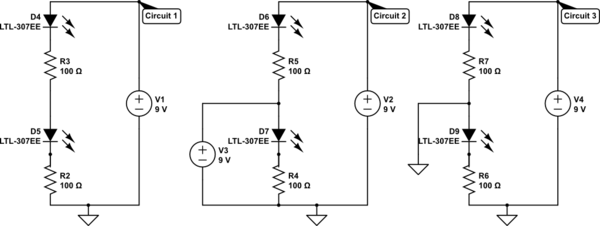
Your circuit redrawn is circuit 1 and there are two possible states circuit 2 and circuit 3.

Circuit 2 is the High state of the 555 timer. In this state the voltage across the top led is 0 (9V on anode and 9V on cathode) which means no current flows and the led is off. Meanwhile the bottom led is on because there is a positive voltage across its terminals (9V on anode and 0V on cathode.). This means that current flows from the 555 through the diode to the ground.

Circuit 3 is the Low state of the 555 timer. This state is the opposite of the previous. Now there is a voltage drop across the top diode and no drop across the bottom. This means that the top is on and the bottom is off. The current flows from the 9V source through the top led and into the 555.

schematic

simulate this circuit – Schematic created using CircuitLab

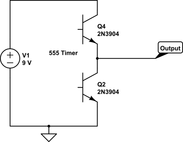
The internal circuitry of the 555 output pin is essentially this:

schematic

simulate this circuit

\$\endgroup\$
0
0
\$\begingroup\$

Think of this from the LEDs POV, when the output is high, LED1 has a a potential difference of 0 between its 2 pins and LED2 has a potential difference of 9V, and vice versa for when the output is LOW, the Potential difference for LED1 is 9V and for LED2 is 0V. How this works internally is that for making the output low, ne555 connects its output to ground, so the current flow into the IC at that point

\$\endgroup\$
9
  • \$\begingroup\$ I've ignored the resistor voltage drop to simplify the analogy, FYI \$\endgroup\$
    – Adi
    Commented Jan 4, 2021 at 19:23
  • \$\begingroup\$ but what would the current flow look like , i understand there is a voltage difference , when the top LED in diagram has potential difference , the current should flow somewhere right ??? \$\endgroup\$ Commented Jan 4, 2021 at 19:26
  • \$\begingroup\$ It would flow into the IC, if you see the internal schematics of any GPIO on any controller, the mechanism is this: to make the output high, a switch connects the output pin to VCC, to make the output pin LOW, a switch connects the output to GND. So the current flows into the IC at that point. \$\endgroup\$
    – Adi
    Commented Jan 4, 2021 at 19:28
  • \$\begingroup\$ so u mean to say that when there is voltage difference between Vcc and pin 3 between the top LED , the current flows through led and then inside through pin 3 , passing the push pull amplifier and then to the discharge and then to ground ?? \$\endgroup\$ Commented Jan 4, 2021 at 19:32
  • \$\begingroup\$ If you see the internal schematics of a ne555, you see a output driver which is a not gate. Now look up how not gates are implemented in VLSI, it consists of a 2 transistors, if you activate the bottom one, the output is grounded. Current flows through this transistor to GND. \$\endgroup\$
    – Adi
    Commented Jan 4, 2021 at 19:36

Your Answer

By clicking “Post Your Answer”, you agree to our terms of service and acknowledge you have read our privacy policy.

Not the answer you're looking for? Browse other questions tagged or ask your own question.