0
\$\begingroup\$

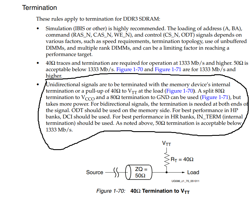
I want to use a DDR3 RAM in conjunction with a FPGA. The FPGA will control the DDR3 RAM. I am using a XILINX 7series FPGA. XILINX has a guide for this, on p.129 is the needed termination mentioned, this can also be seen in below image.

enter image description here

Point 3 states that unidirectional signals need a 40Ohm VTT termination. And bidirectional signals need the termination at both ends. I have a DDR3 memory with an option for a on die termination. So when I use this on die termination do I still need the VTT termination?

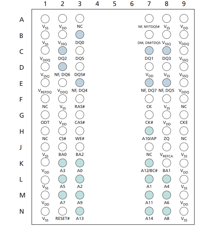
The DQ Pins (data) are bidirectional so I will need a termination at both ends. All other pins are unidirectional, right? So they will just need a termination at the receiver side.

enter image description here

\$\endgroup\$
3
  • \$\begingroup\$ If you have an option for on-die termination, that should cover that side and no extra termination should be required. Transmission lines obviously work best if source, line and sink impedance match, but if you don't have a driver with the right internal impedance, adding a resistor close to the IC only adds another discontinuity and doesn't gain you anything as the reflection from the other side should be minimal anyway due to the termination on that end -- and if you have a driver with the right impedance, then you don't need an external resistor anyway. \$\endgroup\$ Commented Feb 7, 2021 at 22:56
  • \$\begingroup\$ (assuming the On-Die termination is he correct value. Or you aren't clocking the DDR3 interface above 667 MHz) \$\endgroup\$
    – user16324
    Commented Feb 8, 2021 at 11:50
  • \$\begingroup\$ Did the answer solve the problem? What should I do when someone answers my question? \$\endgroup\$ Commented Mar 23 at 18:04

1 Answer 1

1
\$\begingroup\$

Normally the data groups (DQx, DQS, DM) have on die termination, the address and control pins however will need termination to VTT (Check the memory datasheet for details). Note that for DDR3, address and control is normally routed flyby where the data groups are point to point.

Usually the FPGA can handle the source end of the termination if you pick the correct IO banks or let the MIG do it for you, so you just wind up needing a mess of resistors to VTT on the address and control lines.

Note that the VTT plane is the reference for the impedance calculations most of the time, if referencing to other planes (Gnd) you will want extensive capacitive stitching to VTT.

\$\endgroup\$

Your Answer

By clicking “Post Your Answer”, you agree to our terms of service and acknowledge you have read our privacy policy.

Not the answer you're looking for? Browse other questions tagged or ask your own question.