0
\$\begingroup\$

Here is a link to a Falstad simulation:

Link to simulation 1

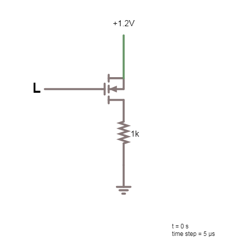
Image of circuit from simulation 1

The NMOS is connected to the VDD, but when it is turned off we have VSD=0,435 V. Why is the drop not 1,2 V?

The reason I don't understand this is that when the NMOS is off, we are not able to attract any electrons from the p-substrate in the NMOS, so how does it not completely shut the current off and we have a voltage drop of 1,2 V, instead of 0,435 V?

When we swap the drain and source in the NMOS the drop will be 1,2 V, why does it then work?

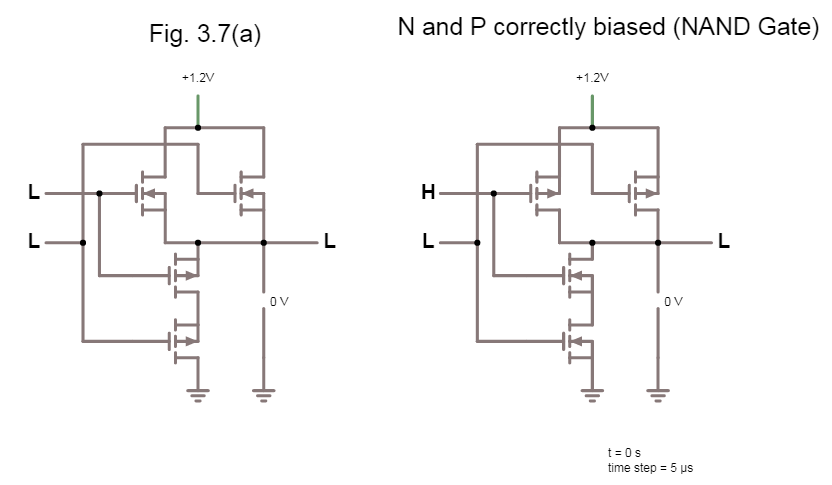
Here's another simulation:

Link to simulation 2

Image of circuits from simulation 2

Look at the left case. Here when the two NMOS on top are turned off, they have an intermediate voltage drop, but here it doesn't matter where the drain and source are?

\$\endgroup\$
4
  • \$\begingroup\$ You have reversed S and D, to forward bias the body diode. \$\endgroup\$
    – user16324
    Commented Feb 15, 2021 at 23:22
  • \$\begingroup\$ This question is basically a repeat of your last question. If your trying to understand your first question using this simulation, it wont work. The transistors in your first question are not connected like this, they have detached body contacts which are connected in a way that ensure body diodes stay off. \$\endgroup\$
    – MAM
    Commented Feb 15, 2021 at 23:43
  • \$\begingroup\$ So while the answers on this post are correct, the body diode stuff do not apply to your original posted circuit. Be careful. \$\endgroup\$
    – MAM
    Commented Feb 15, 2021 at 23:45
  • \$\begingroup\$ @AdilMalik Thank you very much for warning me. So in the second simulation do we also not get the body diode problem? The second simulation gives the same answer if we swap the drain and souce at the NMOS. \$\endgroup\$
    – user394334
    Commented Feb 16, 2021 at 0:44

1 Answer 1

4
\$\begingroup\$

You have connected the NMOS transistor upside down. You have the source connected to the higher voltage, which causes the parasitic diode structure to be forward biased. Flip the transistor vertically.

In your second schematic, left side, you are using NMOS transistors to pull the output high. Since the gate voltage can't get any higher than the drain voltage, the source voltage can only rise until \$V_{GS} \approx V_{TH}\$. As many students have learned, you really can't make a non-inverting gate by using NMOS to pull high and PMOS to pull low.

\$\endgroup\$
11
  • \$\begingroup\$ Hello thank you. Does this mean that the voltage does not go through the source, but goes through the substrate to the drain? \$\endgroup\$
    – user394334
    Commented Feb 15, 2021 at 22:34
  • \$\begingroup\$ Yes, One terminal (the source) has an ohmic connection to the body, which creates a PN junction between the p-type body and the n-type drain. Try to make the source voltage higher than the drain voltage and this diode conducts. Actually, the whole notion of "source" and "drain" breaks down when you connect the transistor upside down like this. \$\endgroup\$ Commented Feb 15, 2021 at 22:36
  • \$\begingroup\$ Thank you, but could you please explain the sentence "Since the gate voltage can't get any higher than the drain voltage, the source voltage can only rise until VGS≈VTH ." Why is it that we have this bound on VGS, why can not VGS be higher?(or "lower" instead of "higher" because I think VGS is - VTH.) \$\endgroup\$
    – user394334
    Commented Feb 15, 2021 at 23:26
  • \$\begingroup\$ \$V_{GS}\$ is the actual voltage from gate to source while \$V_{TH}\$ is a characteristic of the transistor itself. If you use an NMOS to pull up in a logic gate then the transistor's drain will be connected to the supply voltage. If the logic gate input is coming from other logic gates then that signal will also go no higher than \$V_{DD}\$. For the transistor to conduct, \$V_{GS} \approx V_{TH}\$, so the voltage at the source must be less than the gate voltage, meaning less than \$V_{DD}\$. The output can't rise to \$V_{DD}\$. \$\endgroup\$ Commented Feb 15, 2021 at 23:38
  • \$\begingroup\$ But in our case we have that \$V_G=0V\$, \$V_D=1,2V\$ and \$V_S=0,7V\$ and we have set \$V_{TH}=0,7V\$, so we have that \$V_S>V_G\$, and \$V_{GS}=V_G-V_S=-0,7V=(minus)V_{TH}\$. I understand that when the gate has 1,2 V, we wont get out 1,2 V at the source, the problem is that when the gate is 0 V, why we wont get 0 V at the souce? \$\endgroup\$
    – user394334
    Commented Feb 16, 2021 at 0:41

Your Answer

By clicking “Post Your Answer”, you agree to our terms of service and acknowledge you have read our privacy policy.

Not the answer you're looking for? Browse other questions tagged or ask your own question.