Circuit Cellar-Issue 210- has this question "Which connection(s) to a decoupling capacitor should be shortest?why?" in its "Test your EQ section". I couldn't understand what they meant 'Which connection(s)'. Can somebody explain this?
4 Answers
First let's look at what a bypass capacitor is good for. Let's talk about digital circuits, like discrete logic, or an FPGA or a microcontroller. Contrary to what's been said in comments, in many many cases it is a pretty good assumption that the output drivers are the dominant source of power supply switching noise. Exceptions could be very high-end microprocessors or very large FPGAs.
For traditional logic designs it generally also is reasonable to assume capacitive loads. If your outputs are driving transmission lines, you've got some other issues to worry about, but it won't actually change the results of the analysis much.
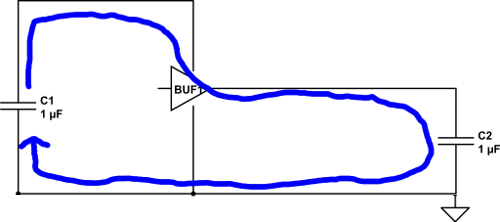
Let's say an output driver is switching from low to high. Then the high frequency components of current flow basically as shown in this diagram:

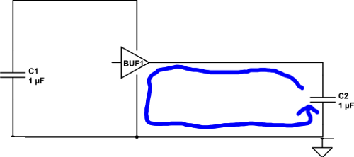
When the output is switching from high to low, the high frequency components of current flow basically like this:

I've put the reference ground down at the end of the line because that's where the receiver will be trying to decide between a '1' and a '0', so that's where the noise margins will matter.
First thing to notice is the bypass capacitor doesn't have much to do with what happens for 1-0 transitions. We'll leave the issue of ground bounce for another question.
Second thing is that for the 0-1 transitions, the current path goes from the capacitor to the driver, and it comes back to the capacitor from the signal's return path. So in this case, what's critical is the path from the capacitor to the driving chip's Vcc pin, and from the ground plane (you are using a ground plane, right?) to the capacitor.
Of course if you're doing analog filters, or power, or something else, you should look for the current loops and do an analysis of your specific situation to know how to optimize your bypassing layout.
For reference, here's the original answer to the question:
The most important connection is between the supply side of the capacitor and the supply pin of the chip.
The biggest transient currents in most integrated circuits are related to the switching of the output pins. When a pin switches from low to high, a pulse of current is drawn from the chip's external supply to charge the output node, which includes the capacitance of the PCB trace and the input gate of the next chip. This current is primarily supplied by the decoupling capacitor.
Note that this current "returns" to the ground end of the capacitor NOT by way of the same chip's ground pin, but rather by way of the PCB ground plane and the ground pins of the chip(s) that it is driving. For this reason, it is not particularly important that there be a short ground connection between the driving chip and its capacitor, but it is important that the capacitor be bonded as directly as possible to the PCB ground plane.
When an output switches from high to low, the capacitance of the output node must be discharged, which causes another pulse of current. However, this pulse does not involve the decoupling capacitor at all. Instead, it flows from the capacitance of the output node, through the pulldown transistor and into the ground plane, where it is "returned" to the other end of the distributed node capacitance. This is why the ground pins of all chips need to be be bonded as directly as possible to the PCB ground plane.
If any part of this is not clear, I'd be happy to expand on it as needed.
-
\$\begingroup\$ Wow, they're making a HELL of a lot of assumptions there. 1: You have a ground-plane. 2: The switching transients are caused by the chip driving capacitive loads, rather then the IC's internal operations. \$\endgroup\$ Commented Jan 14, 2013 at 19:29
-
2\$\begingroup\$ Basically, except in a few, specific cases, their "answer" is mostly bullshit. If you're doing analog, it's completely bullshit. \$\endgroup\$ Commented Jan 14, 2013 at 19:29
-
\$\begingroup\$ @ConnorWolf -- Chapter 10 in Electromagnetic Compatibility Engineering discusses this topic in gory detail; as to the answer here -- it's fairly incomplete. \$\endgroup\$ Commented Feb 8, 2015 at 1:40
In an ideal world both of the leads of the decoupling capacitors should be as short as possible and be as close to the IC supply pins as possible.
Now that said, with many logic chips using threshold specifications following the old TTL standard where the noise margins near ground are less than those near the VCC or VDD then it is desirable use extra care to keep down noise on the GND bus. Thus if you have a non-ideal condition and it is necessary that the bypass capacitor has a tradeoff of where one connection has to be longer than the other then it will be appropriate to favor the shorter connection at the GND side of the capacitor.
If a circuit used all CMOS type logic thresholds where the noise margins at GND and VDD are the same then it may be best to try to even out the bypass capacitor connection length on both sides.
You want to make both connections as short as possible; if you can't make them short, an acceptable alternative is to "zigzag" the power and ground routes to the capacitor instead of using T-traces to "stub" the connection in. This puts the inductance of the trace in series with the power trace, where it can act to suppress noise, instead of in series with the capacitor, where it just acts to render the capacitor a less effective filter.
