2
\$\begingroup\$

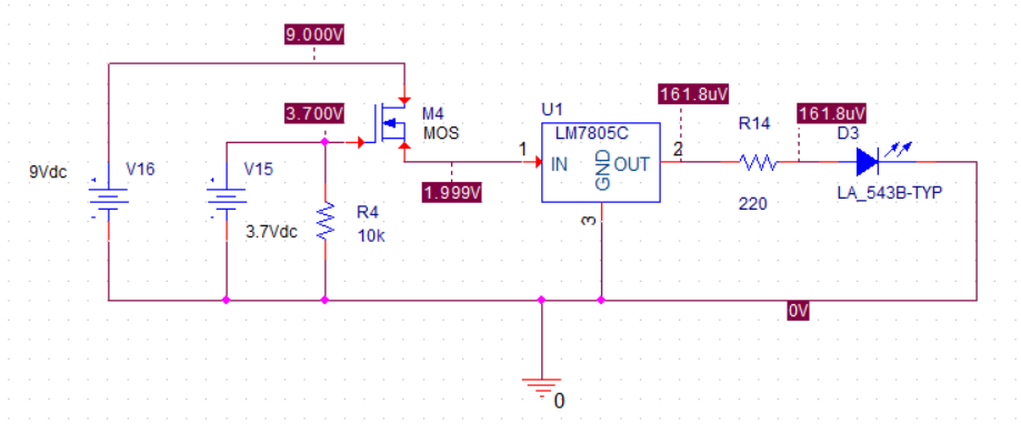
I initially designed a circuit with a P55N06 MOSFET that would be used with a LM7805. The drain is fed by 9V, the source connects to the 'in' pin of the LM7805 and the gate is fed by 3.7V. The simulation results for this are:

enter image description here

I expected to get 9V on the source, but as you can see it's only 2V. Any ideas on what I'm doing wrong here?

\$\endgroup\$
2
  • \$\begingroup\$ You need P-MOSFET. \$\endgroup\$
    – user263983
    Commented Mar 7, 2021 at 2:58
  • \$\begingroup\$ Can you give me an insight on how the circuit would look like? Sorry, I don't really know much of type-P MOSFETs. \$\endgroup\$
    – gabslks
    Commented Mar 7, 2021 at 3:01

3 Answers 3

4
\$\begingroup\$

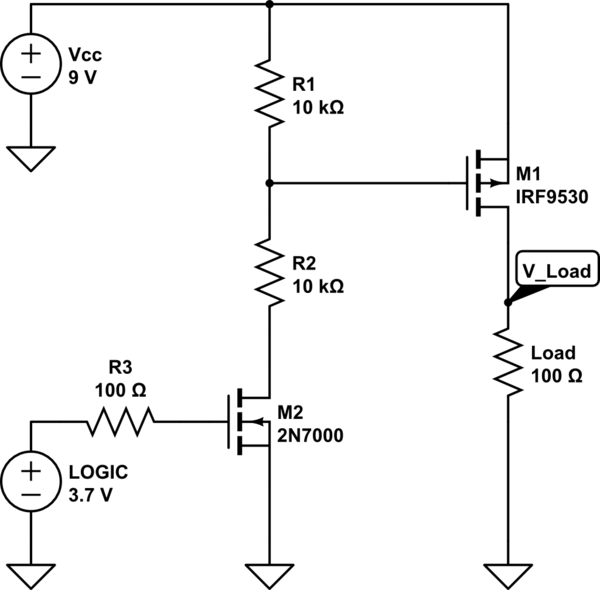
The circuits you linked in your comment are correct in general. If you still don't get the expected results you may need to select different components or check if the components have the right orientation. Below is an example circuit with suitable MOSFETs.
schematic

simulate this circuit – Schematic created using CircuitLab

Just like a N-type, the P-type conducts when there is a sufficiently large potential difference between the source and the gate terminal, but with reversed polarity (note the orientation of the high-side pMOS). Respectively, to "turn off" the MOSFET, base and source must be on the same potential. In your example you have to bring the gate of the pMOS up to 9V, which is far above your logic level.

In case the voltage to switch is higher than the logic level, a nMOS can be used to drive the gate of the pMOS. When a logic high is applied at the nMOS' gate, the nMOS (=low-side switch) pulls the gate of the pMOS to a desired level (in the example a 50:50 divider is used to get 4.5V) - the "switch is closed". Respectively, the "switch is open" on a logic low.

R2 is only required if the supply voltage exceeds the maximum rating for the gate-source voltage of the pMOS. The IRF9530 is rated for Vgs,max=20V, so pulling the gate down to GND directly would work, but in some cases, a voltage divider is required. The purpose of R3 is to limit the current required to charge the nMOS' gate capacitance. As a rule of thumb, suitable MOSFETS should have a gate-source threshold voltage (Vgs,th - the voltage at which the device starts to conduct) of no more than half the voltage that is actually used to drive the gate. Though, the nMOS is not very critical in this case, a 2N7000 works.

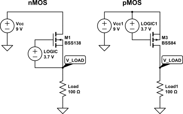
An alternative approach using only one MOSFET is this:
schematic

simulate this circuit

Here, MOSFETS with low Vgs,th are chosen. Note: the logic level circuitry and the load do not share a common ground in those cases, which means you can easily fry things. The first example does not have this problem, though.

\$\endgroup\$
2
  • \$\begingroup\$ This solves the problem completely! Thank you for taking the time not only to draw the possible solutions, but also to explain why it works. It is really helpful! \$\endgroup\$
    – gabslks
    Commented Mar 8, 2021 at 1:34
  • \$\begingroup\$ As for the circuit, even after you posted this answer I still wasn't able to turn the switch off. After some time trying to find where the problem was I realised that I had swapped the drain and the source of the P-type mosfet. The source pin on the simulator I'm using is located at the bottom of the mosfet, while the examples I found (and your answer) have the source at the top. \$\endgroup\$
    – gabslks
    Commented Mar 8, 2021 at 1:34
1
\$\begingroup\$

I believe there's some misunderstanding here. FETs act as resistors (i.e. switches) when there's full inversion in the channel.

We're usually taught to think that as long as VGS > VTH there will be a channel. But this about what your VG and your VS are since VGS = VG - VS. VG is 3.7V supply but VS is at a high impedance node (i.e. undefined). If you want your FET to operate as a switch, you need pull that gate to supply for NMOS or to GND for PMOS to achieve the inversion on the channel.

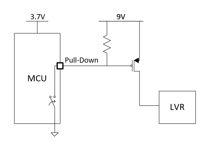
I'll assume you have the 3.7V supply because you want to control this with a logic signal. In that case I recommend using a PMOS device. This turns your enable into an active low. It's funny because these kind of questions come up on technical interviews for electrical engineers. It'll look something like this, provided that your MCU can handle the 9V at the IO pin.

enter image description here

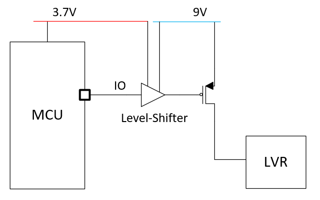
One thing to consider is the exposure of the IO pin to 9V during the pull-up condition. Therefore, a level-shifter (level translator) could be used instead, if your IO pin cannot handle 9V.

enter image description here

\$\endgroup\$
0
0
\$\begingroup\$

The switch FET needs a gate sot source voltage of many volts to turn on.

It will need a drive of >12V, not the 3.7V you are giving it.

Look into "high-side drivers".

\$\endgroup\$
2
  • \$\begingroup\$ Isn't the purpose of using MOSFETs as switches the possibility to put a low voltage on the gate and pass a high voltage from drain to source? For this reason I chose the P55N06, as this MOSFET has a low Vth that would enable me to have only 3.7V on the gate. \$\endgroup\$
    – gabslks
    Commented Mar 7, 2021 at 2:43
  • \$\begingroup\$ 3.7V between source and gate, not between source and ground. \$\endgroup\$
    – user263983
    Commented Mar 7, 2021 at 3:00

Your Answer

By clicking “Post Your Answer”, you agree to our terms of service and acknowledge you have read our privacy policy.

Not the answer you're looking for? Browse other questions tagged or ask your own question.