1
\$\begingroup\$

I want to design a high side load switch which can allow or block DC current in either direction based on a 3.3V input.

Some considerations:

  1. The 3.3V rail is potentially created as a result of power being applied on either side of this switch, so with the thought that the 3.3V rail may still be coming up, the switch should be open (blocking) with it not present.

  2. I would like to switch voltages up to 20VDC.

The circuit that I have currently looks like this:

Current circuit

This works with some caveats:

  1. Some current passes through for about 10ms when power is applied. I'm not sure I completely understand why but I'd like to mitigate/remove that. For it to be that long, it would seem to not be related to the switching time of the MOSFETs, and swapping the 100k resistors for 1k didn't change it.

  2. For switching 20V, I need to select P-FETs where Vgs can be 25V or greater, which limits my parts selection. This is not the end of the world but maybe there's a better way to do it.

How can I improve this circuit, use smaller/cheaper/fewer parts, and mitigate the caveats above?

This is ultimately part of a USB C power mux circuit as I mentioned in my previous question, so ideally I want to be able to have two of these and open one, or the other, or neither, but never both at the same time (because then 20V may end up on my VBUS rail and that's no good for anyone). This may be out of scope for this question but I provide this info to avoid the XY problem.

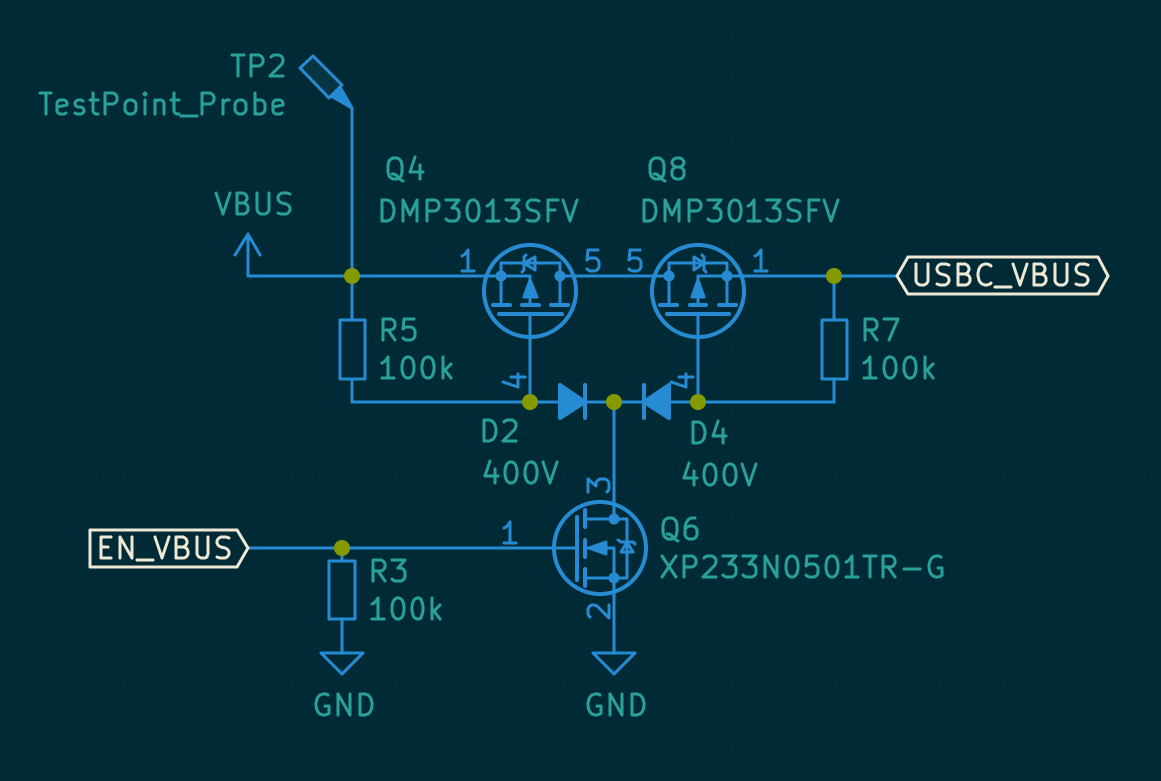
\$\endgroup\$
4
  • \$\begingroup\$ Your Vgs is likely to exceed the maximum tolerable when pulling the gate low. You need to limit it if you plan on running it with a sufficiently high Vdd. No need to find a part where Vgs can be higher than 25V. You are unlikely to find one. \$\endgroup\$
    – DKNguyen
    Commented Apr 14, 2021 at 2:37
  • \$\begingroup\$ The part listed on the schematic can do it, but I see what you're saying that the part selection is sparse. I suppose I can put another 100k resistor at the drain of the N-FET so I'd have -10Vgs for 20V and -2.5Vgs for 5V, which is still enough to drive into saturation on the low end. \$\endgroup\$
    – Paulywog
    Commented Apr 14, 2021 at 2:45
  • \$\begingroup\$ You would normally use a zener diode to limit how close Q6 can pull to GND. In this case it looks like you would need two, and you would still need the drain resistor to limit current through them. A bit more parts, but also more reliable (or at least independent of Vdd) than just halving Vdd. \$\endgroup\$
    – DKNguyen
    Commented Apr 14, 2021 at 2:45
  • \$\begingroup\$ notice how many important specs are in LTC4418. these are what’s expected to design it yourself with tolerances on what counts. Learn to remember these categories when designing in future a write a spec first on sequencing, latency, thresholds, losses etc. Just a suggestion for improving design skills \$\endgroup\$
    – D.A.S.
    Commented Apr 14, 2021 at 3:29

1 Answer 1

1
\$\begingroup\$

One way to check your design is to see how the pro's do it. Linear Technology (now a part of Analog Devices) has a line of power path controller chips that drive external power MOSFET's. To be fair, some use your arrangement with the two drains connected. but most have the two sources connected. This eliminates the need for D2 and D4, so there is more gate voltage for enhancement.

Here is a link to one of their datasheets. The circuit on the front page shows the FET connections.

https://www.analog.com/media/en/technical-documentation/data-sheets/ltc4418.pdf

\$\endgroup\$
2
  • \$\begingroup\$ Thank you! As I believe is typical for LT/AD, that chip looks like the perfect solution... but costs nearly $6 per. As a learning tool though I think it will be invaluable. So as @DKNguyen was saying I'd use a zener to clamp. Then with the sources connected, I can lose the external diodes. My only remaining question is why my current circuit leaks some current for the first 5-10ms, and how to prevent that. \$\endgroup\$
    – Paulywog
    Commented Apr 14, 2021 at 3:14
  • \$\begingroup\$ Have you scoped the EN_VBUS signal during that time? \$\endgroup\$
    – AnalogKid
    Commented Apr 14, 2021 at 12:10

Your Answer

By clicking “Post Your Answer”, you agree to our terms of service and acknowledge you have read our privacy policy.

Not the answer you're looking for? Browse other questions tagged or ask your own question.