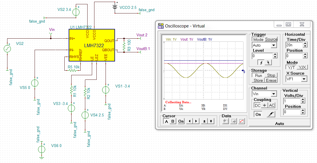
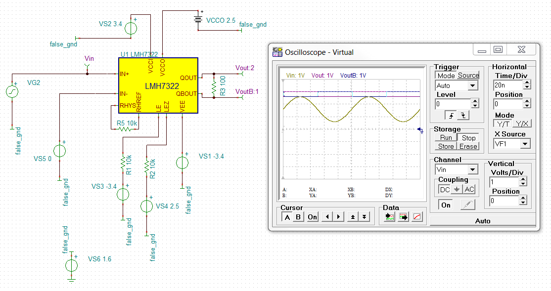
I'm having trouble with a comparator from TI (LMH7322). I use it in the circuit shown in the attached image "Comparator_1" .
.
Outputs go to an FPGA. The circuit is supposed to take a single ended input signal (VG2), which is between +/- 1V at up to 80MHz, and turn it into an LVDS signal. The TINA simulator gives a constant output in the configuration shown (1.4V on VoutB and 1.0V on Vout). In reality, both Vout and VoutB are at 1.8V, with noise at a frequency matching the input (VG2) frequency. I thought the simulator was wrong and I found that shifting all voltages up by 1.6V (as in "Comparator_2" ) makes the simulator work (note the "false_ground" net and VS6 voltage).
I therefore think the simulator has a problem.
The outputs QOUT and QBOUT The datasheet for the part (LMH7322 datasheet) states that QOUT and QBOUT should have levels VCCO-1.5V and VCCO-1.1V or VCCO-1.1V and VCCO-1.5V. Note that my setup is as per the datasheet's Figure 11 with VCCI and VEE set to +/-3.4V respectively.
So I have two questions: Do you agree that the issue shown by the simulation is really a problem with the simulation model? Why would the outputs of the comparator be both at 1.8V rather than 1.0V or 1.4V?
Edit: The outputs go straight to the FPGA pins and the termination resistor (R3) is close to these pins. The FPGA is an Altera Cyclone IV. The FPGA pins are on a bank whose I/O voltage is 2.5V (as required for LVDS on this FPGA) and the pins are set as LVDS inputs.
