0
\$\begingroup\$

schematic

simulate this circuit – Schematic created using CircuitLab

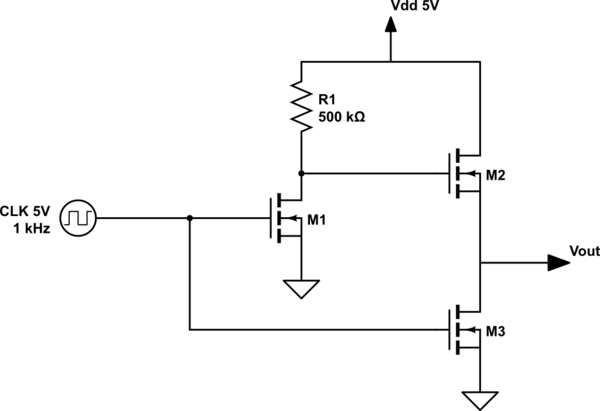
I am trying to design a buffer only using NMOS and resistor as this picture shows. The goal is to get the CLK signal as much amplitude as possible. My questions are maybe little too basic, so

  1. How can I ensure that?
  2. Generally speaking, how to design a good buffer? What kind of aspects should I be concerned about?
\$\endgroup\$
7
  • 6
    \$\begingroup\$ 'As much amplitude as possible' is not a specification. What's the clock frequency? The power supply voltage? The required rise time? The load? \$\endgroup\$
    – Neil_UK
    Commented Apr 29, 2021 at 17:02
  • \$\begingroup\$ I mean trying the maintain the clock amplitude through the buffer, the load can differ \$\endgroup\$
    – 0XY0
    Commented Apr 29, 2021 at 17:13
  • \$\begingroup\$ You need some kind of charge pump to keep M2 fully on. And probably a decent dead-time system. There's half-bridge gate driver IC's with bootstrapping that do all of this for you... \$\endgroup\$ Commented Apr 29, 2021 at 17:14
  • 1
    \$\begingroup\$ how to design a good buffer? By studying to become a circuit designer, yeah I know, "stupid" answer. The thing is, "how to design a good buffer" isn't a good question here, it is too broad. We can't tell you "how to design a circuit" in an answer here. \$\endgroup\$ Commented Apr 29, 2021 at 17:23
  • 3
    \$\begingroup\$ At the risk of being redundant: "good" does not invoke a specific figure of merit, and some figures of merit conflict directly with others. Does good mean low-power? Does good mean fast? Does good mean reliable? Does good mean low-cost? Does good mean easily-analysed? \$\endgroup\$
    – Reinderien
    Commented Apr 29, 2021 at 17:38

1 Answer 1

2
\$\begingroup\$

what kinda aspects should I concern about?

One thing you should be concerned about is "shoot-through". Shoot-through occurs when two stacked transistors, such as those in your circuit, are both conducting, forming a low impedance path between the power supply rails. Since this is a low impedance path, significant currents may flow during shoot-through.

Although integrated circuits may have mosfet's "stacked" as you have done, the designers of those circuits either ensure, or require the user to ensure, that the transistors are never never both on simultaneously, or, if that can't be guaranteed, that the overlap when both transistors are conducting simultaneously is relatively short.

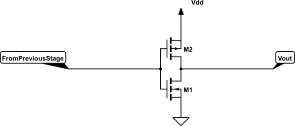
One way to ensure that only one MOSFET is conducting at a time, or if both are conducting, it is only for a brief moment, is to use complementary MOSFETs with a threshold voltage that is more than half of the supply voltage, and tie the gates together. The use of complimentary MOSFETs simplifies driving the gate of the upper transistor.

The output stage of your buffer could then look like this.
schematic

simulate this circuit – Schematic created using CircuitLab

With such a design, the supply voltage and the MOSFETs' threshold voltages MUST be designed to be compatible. Shoot-through could easily destroy the transistors.

Remember, this circuit is the output stage of your buffer only. Stand-alone, it is a logical inverter.

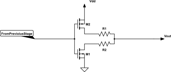
An alternative approach, that works for MOSFETs with "low" threshold voltages is to include 1 or 2 resistors between the MOSFETs in your output stage, perhaps like this:
schematic

simulate this circuit

This circuit is also a logical inverter made from discrete MOSFETs.

The resistors R1 and R2 reduce shoot-through current to what may or may not be reasonable levels for your application. Increasing their value will reduce shoot-through current, but will also reduce the current available for output (i.e. increase the output impedance). Conversely, decreasing their value will reduce the output impedance, but will increase the shoot-through.

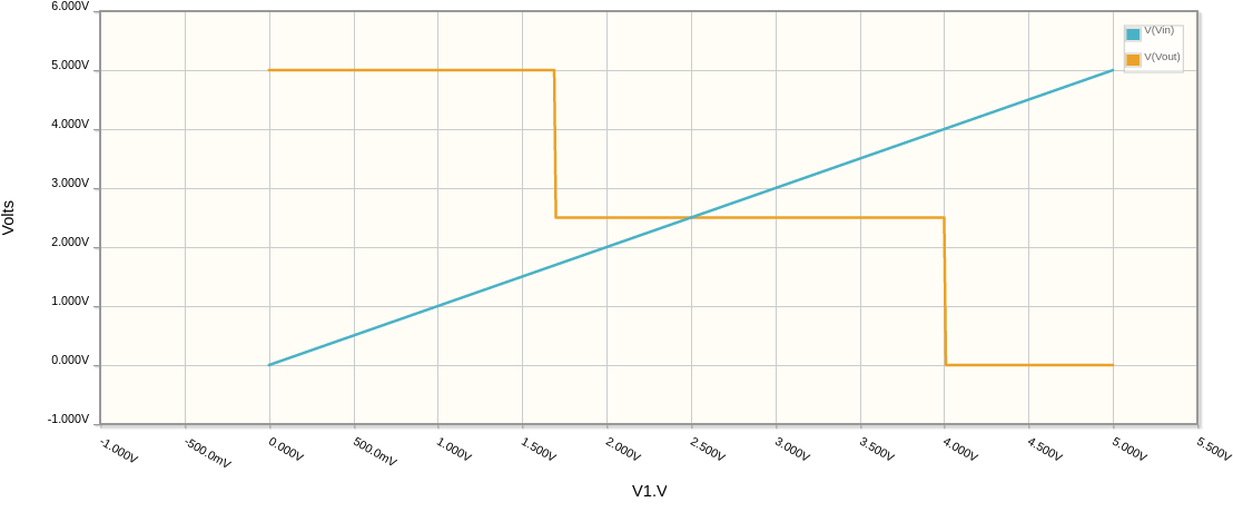
The input/output characteristics of this circuit may look something like this if the MOSFET threshold voltages are low:
enter image description here

If the resistors have equal values, then when both transistors are equally "on", the output will be about half of Vdd. This can be modified by changing the values of those resistors. [One resistor may be omitted entirely]. Changing the resistor ratio will affect the ratio of sink to source current for high and low outputs.
\$\endgroup\$
7
  • \$\begingroup\$ Wouldn't putting the two 10k resistors in series with the output put some pretty big restrictions on the load driving capability, and thus the max amplitude? I completely agree about shoot through when using stacked transistors and the resistors do solve that, but it makes the output a relatively high impedance. \$\endgroup\$
    – Aaron
    Commented Apr 29, 2021 at 19:40
  • \$\begingroup\$ Yes, it makes the output a relatively high impedance. One can use smaller resistors, get a lower output impedance, but greater shoot-through. One can add more complexity to get around this, but at some point, the complexity is such that it doesn't make sense to use discrete components, but to use someone's well-designed IC. \$\endgroup\$ Commented Apr 29, 2021 at 19:45
  • \$\begingroup\$ How to avoid through current? Question was about " good" buffer \$\endgroup\$
    – user263983
    Commented Apr 29, 2021 at 20:12
  • \$\begingroup\$ @user263983 I'm not sure I understand your question? How to avoid shoot-through current? I showed two methods. 1) Use MOSFETs whose threshold voltage is more than 1/2 Vdd. 2) Use resistors between the MOSFETs. There are other ways as well, but more complex. Could you clarify what you are asking? Did I answer you already? \$\endgroup\$ Commented Apr 29, 2021 at 20:15
  • \$\begingroup\$ Yes, it is OK. Just to find right MOSFET. \$\endgroup\$
    – user263983
    Commented Apr 29, 2021 at 20:17

Your Answer

By clicking “Post Your Answer”, you agree to our terms of service and acknowledge you have read our privacy policy.

Not the answer you're looking for? Browse other questions tagged or ask your own question.