0
\$\begingroup\$

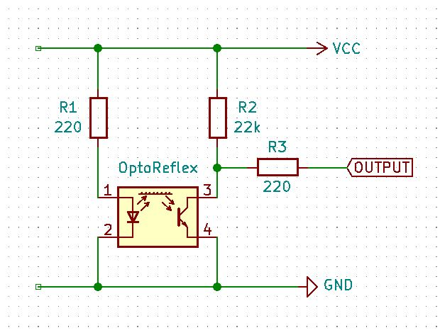
I'm currently working on a phototransistor that is part of a reflective optical sensor. Now I saw a circuit, which looks like this and I'm wondering why there is the (additional) resistor \$R_3\$ ?

enter image description here

In my understanding the usual phototransistor circuit is a voltage divider between \$R_2\$ and the resistance of the transistor (i.e. low illumination \$\propto\$ high resistance and bright illumination \$\propto\$ low resistance). Then the analog output of the circuit will read a value between \$VCC\$ and almost zero (determined by the dark-current).

However, here I cannot explain to myself why we have the resistor \$R_{3}\$ in front of the analog out?

Thanks for your help!

\$\endgroup\$
3
  • \$\begingroup\$ Can you add details of the application, where this circuit is from, what the opto' does and the load. \$\endgroup\$
    – TonyM
    Commented Apr 30, 2021 at 9:47
  • \$\begingroup\$ I found it as part of a 'line follower' evaluation kit: arrow.com/en/reference-designs/… Thus, the load is connected to a MCU. \$\endgroup\$
    – JoS
    Commented May 3, 2021 at 5:59
  • \$\begingroup\$ What about the application: where you'll use it, what will trigger it and how fast? (Please edit new information into your question rather than add it in comments. Otherwise people have to piece together the full question from it all.) \$\endgroup\$
    – TonyM
    Commented May 3, 2021 at 6:15

2 Answers 2

2
\$\begingroup\$

R3 is not required for the functionality of the optocoupler. It is required by the circuitry connected to the OUTPUT. Since we know nothing bout that circuit, we can only guess. It could be there for isolation, short circuit protection, low pass filtering (with the input capacitance of the load), or it sets the DC current on an LED etc.

\$\endgroup\$
2
  • \$\begingroup\$ I like your approach. I'd add +1 if there was more detail about various receiving circuits. As it is, it's too short to meet my own criteria. \$\endgroup\$
    – jonk
    Commented Apr 30, 2021 at 7:39
  • \$\begingroup\$ Indeed, this circuit is just an extension to a more complicated picture and my expectation was already, that R3 is somehow related to the rest. So I was just wondering if there is a good reason on the phototransistor side that R3 exists. Thanks. \$\endgroup\$
    – JoS
    Commented Apr 30, 2021 at 8:11
0
\$\begingroup\$

It is likely that R3 is to limit the photo-transistor current to a safe level.

When the OptoReflex photo-transistor is on (conducting), it will sink current from R2 and OUTPUT down to GND.

If OUTPUT is capable of providing more current than the photo-transistor can handle, it could damage the OptoReflex part. This might happen if a fault shorts OUTPUT to a supply rail, for example.

The R3 value should be chosen to limit to the maximum photo-transistor sink current for a given photo-transistor voltage drop, both of which should be specified in its datasheet.

You don't specify the OUTPUT load or wiring situation so the reasons for 220R can't be seen.

\$\endgroup\$
2
  • \$\begingroup\$ Tony, It's also not atypical for a resistor of this value to be used to dissipate energy so that the probability of oscillation with a MOSFET capacitance is mitigated. The actual fact is that we don't know anything about the receiving circuit. So that's a problem here in really identifying the thinking process for adding it. \$\endgroup\$
    – jonk
    Commented Apr 30, 2021 at 7:37
  • \$\begingroup\$ @jonk, sure but that's nowhere near as typical as DC current limitation. Reflective sensors are interesting, I've used them a good few times in mass production. As you say, we don't know the application so I've modified my answer. \$\endgroup\$
    – TonyM
    Commented Apr 30, 2021 at 9:49

Your Answer

By clicking “Post Your Answer”, you agree to our terms of service and acknowledge you have read our privacy policy.

Not the answer you're looking for? Browse other questions tagged or ask your own question.