0
\$\begingroup\$

SE, I am trying to replicate the F-shape microstrip antenna design shown in: https://www.researchgate.net/publication/330747527_Dual-Band_Monopole_Antenna_for_RFID_Applications

in Keysight's ADS,

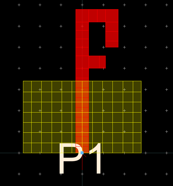
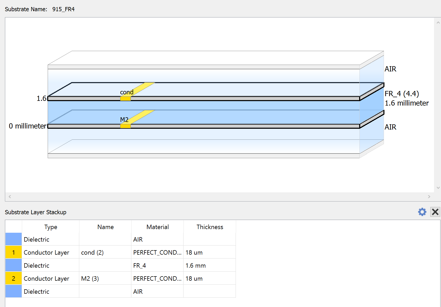
I have set up the substrate and layout to mirror the values used in the paper. The layout is terminated with a 50 ohm pin which represents the SMA 50 ohm connector in the paper. enter image description here enter image description here
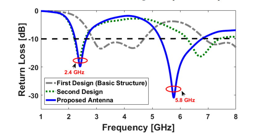
I should expect an S11 plot as shown below: Expected S11
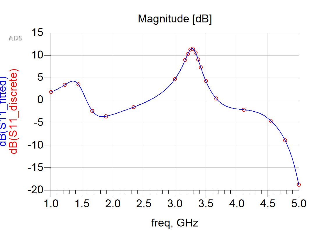
but when I simulate it in ADS, I get

Actual S11

I don't understand why my S11 plot is different if I used the same values and followed the paper verbatim.

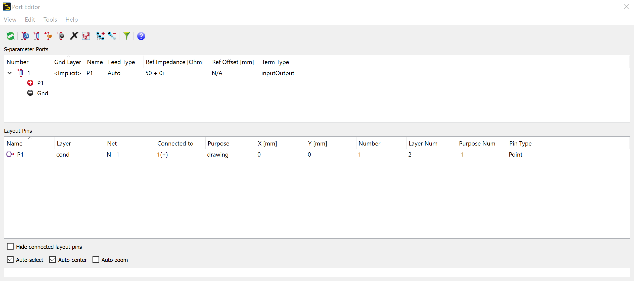
Port Editor

\$\endgroup\$
4
  • \$\begingroup\$ Perhaps post a link to the paper so we can see what you were trying to emulate...? As it stands, you posted a link to a PDF file on your local computer. \$\endgroup\$
    – Shamtam
    Commented May 2, 2021 at 22:48
  • \$\begingroup\$ Fixed. Thanks for letting me know \$\endgroup\$
    – Aaron
    Commented May 2, 2021 at 23:07
  • \$\begingroup\$ The paper you linked to looks like a completely different antenna design. Also, how did you set up your ports in ADS? Show the Layout Port Editor dialog. Your display S-parameters are nonphysical (passive structure shows \$S_{11}\$ greater than 0dB?). I highly suspect your EM port setup is not done correctly (not to mention, the meshing is quite sparse). \$\endgroup\$
    – Shamtam
    Commented May 3, 2021 at 1:50
  • \$\begingroup\$ Yikes! I uploaded the wrong link but I have the correct one now. I also added the port editor but I left port 1 as the default because I wasn't sure what the parameters meant. \$\endgroup\$
    – Aaron
    Commented May 3, 2021 at 3:12

1 Answer 1

1
\$\begingroup\$

Your port setup looks incorrect for the structure you're simulating. Note that your substrate does not have a ground plane, but simply two layers: cond and M2. Your port editor shows that you're using a global Gnd for the negative reference for your EM port (this is what <Implicit> is referring to), which in the case of Momentum for a substrate without a bottom/top cover, uses infinity as the implicit reference.

Try setting the Gnd Layer column to the yellow layer in your layout (I assume that is M2) and re-simulating.

\$\endgroup\$
2
  • \$\begingroup\$ So I changed the <implicit> to cond on the port settings and that worked. I will also try to change the M2 to GND. M2 was my ground layer but I wasn't sure how to set it to ground instead of just making a new layer in the substrate editor. As you can see, I am pretty new to PCB and layout design. Thanks a lot! \$\endgroup\$
    – Aaron
    Commented May 4, 2021 at 0:43
  • \$\begingroup\$ If it is of any consolation, many very experienced microwave engineers also run into reasonably simple issues like this. In my experience, very few circuit designers understand all of the nuances of EM simulators, so issues like this are quite common. Glad to be of help! \$\endgroup\$
    – Shamtam
    Commented May 4, 2021 at 1:56

Your Answer

By clicking “Post Your Answer”, you agree to our terms of service and acknowledge you have read our privacy policy.

Not the answer you're looking for? Browse other questions tagged or ask your own question.