5
\$\begingroup\$

In looking at the AGC schematics, I'm finding a lot of instances where the outputs of some of the NOR gates are tied together when feeding into another gate. The most dramatic example being here, where 4 NOR gates all have their outputs tied together.

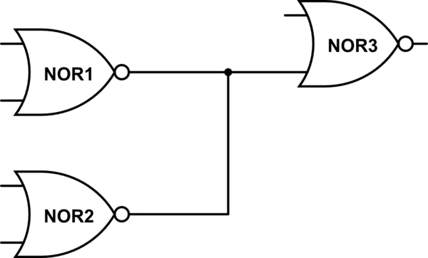
More commonly though, the gates tied together look something like this:

schematic

simulate this circuit – Schematic created using CircuitLab

I can't imagine there'd be a reason for doing something like this in modern digital logic, since it seems like there'd be contention if one gate's output was low, and the other high.

So what's going on here, exactly? My first thought was that maybe it's some kind of "poor man's OR gate," allowing the next gate in the stage to see a high if at least one of the gates is high.

Is there some quirk with RTL logic that would allow it to work this way, or is the reason for this something else entirely?

\$\endgroup\$
1
  • 5
    \$\begingroup\$ RTL luckily lasted a relatively short time. It's "open-collector." Still, even a lot of early TTL used open-collector outputs. Open-collector is useful for multiple-talker situations but was eventually replaced with tri-state (transmission) outputs (for those kinds of bus situations.) \$\endgroup\$
    – jonk
    Commented May 10, 2021 at 20:50

4 Answers 4

21
\$\begingroup\$

RTL logic is open-collector, which allows the wire-OR connection (in this case, more precisely, wire-NOR.) The characteristic of wire-OR is that gates only drive low, so even if more than one is enabled, there is no clash. The gates share a common pullup resistor.

Wire-OR (that is, open-collector or open-drain) is still used. I2C for example is wire-OR. Wire-OR also is used for control signals where multiple devices share the same signal. Example: 'power good' from multiple voltage regulators, or interrupt pins from multiple devices.

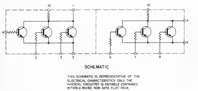
The AGC's NOR IC supports a 'fan in' mode, where they connect the gate outputs without connecting the pull-up. In other words, when they connect multiple gates in wire-NOR, they designate only one to have the pull-up resistor, all the others have their pullup resistors left open. This is done to reduce power, and to ensure that the low-drive loading is kept within spec.

Here's the AGC’s NOR IC pinout:

enter image description here

From here: https://djjondent.blogspot.com/2019/07/the-apollo-guidance-computer-nor-gate.html

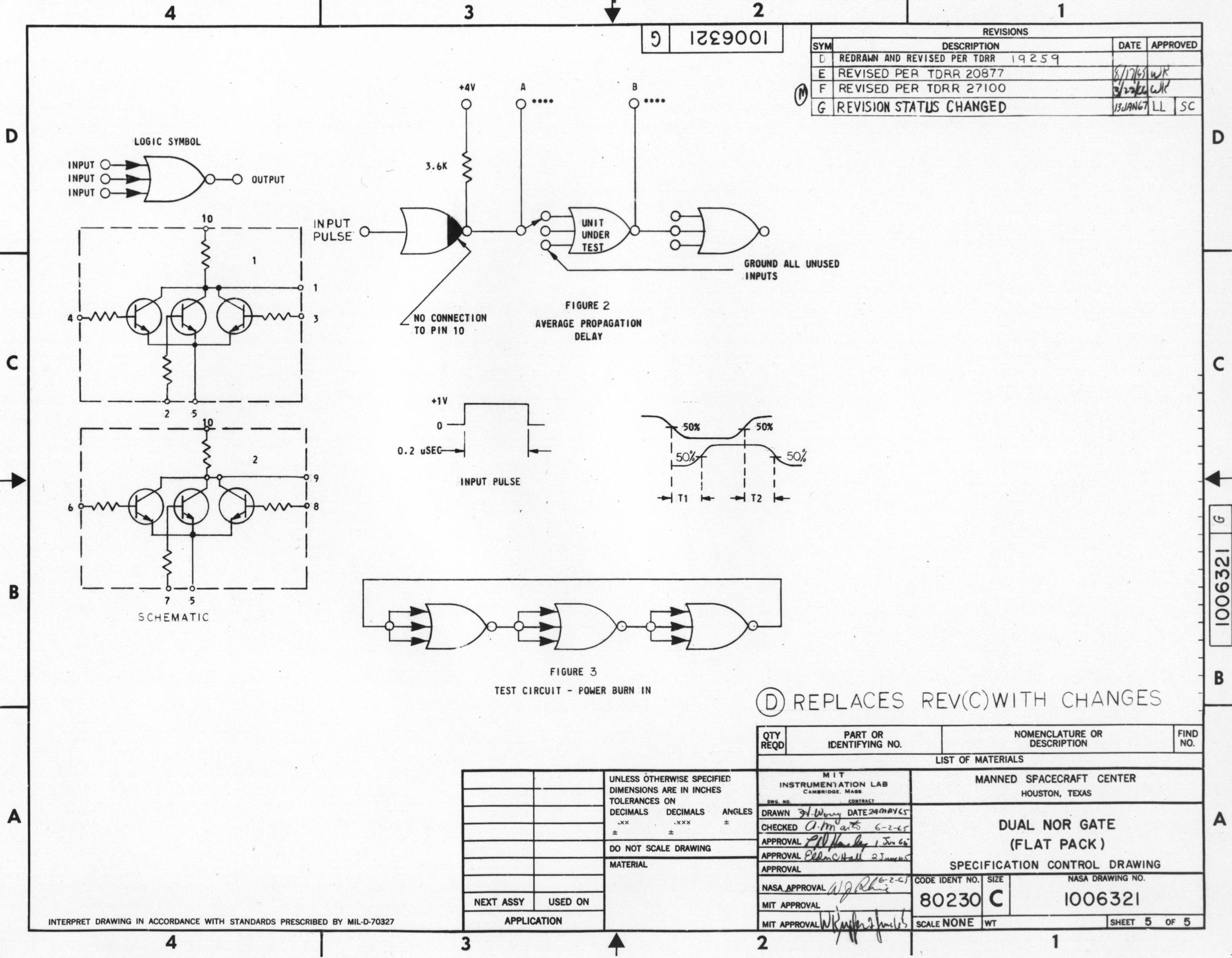
And here's how it's used in a schematic:

enter image description here

From here: http://klabs.org/history/ech/scd/index.htm

Pull-up vs. non-pull up are shown on the AGC schematics as follows:

  • pull-up gate: normal NOR (pin 10 connected.)
  • no-pull-up (fan-in) gate: 'blue nose' shaded output (pin 10 disconnected.)

(Why 'blue nose’? Because... copies from a diazo machine are blue.)

\$\endgroup\$
7
  • \$\begingroup\$ So if I were to draw this schematic in modern TTL instead, I could replace those wire tie points with an extra NOR gate? \$\endgroup\$
    – stix
    Commented May 10, 2021 at 19:58
  • 4
    \$\begingroup\$ Yes, you'd add a gate. Or you could use diodes to 'or' them, a technique I've used for reset circuits. \$\endgroup\$ Commented May 10, 2021 at 20:01
  • \$\begingroup\$ If it's a wire NOR gate though, shouldn't the tied wire be logic high if both gates' outputs are low? How does it get high then if both drivers are low? \$\endgroup\$
    – stix
    Commented May 10, 2021 at 21:37
  • 1
    \$\begingroup\$ Not sure what you're saying here. When all the tied-gate inputs are low, none of the NPN transistors are ON. Then the output is pulled up by the resistor. If any one of the inputs is high, its NPN will pull the line low. \$\endgroup\$ Commented May 10, 2021 at 21:42
  • \$\begingroup\$ @stix, Note that the input signals (voltages) are inverted by the transistors so that when only one of the input voltages is high, the "resistance" (between the collector and emitter) of the corresponding transistor is zero; so the output voltage is zero. Only when both input voltages are low, both transistors are off; so their collector-emitter "resistances" are infinite (open circiit) and the output voltage is high. \$\endgroup\$ Commented May 11, 2021 at 15:58
6
\$\begingroup\$

how is this any more "poor man's logic gate" than all the rest in RTL? Replace your logic gates in your diagram with the actual transistors and resistors, and you'll see that the output of a gate in RTL is "pull-down" logic.

Whenever either NOR1 or NOR2 outputs "low", the common node is pulled towards ground. This is a NOR gate, the way it's usually implemented in RTL, as far as I can tell.

\$\endgroup\$
0
\$\begingroup\$

@hacktastical's answer covers the fundamentals, but there are some more points:

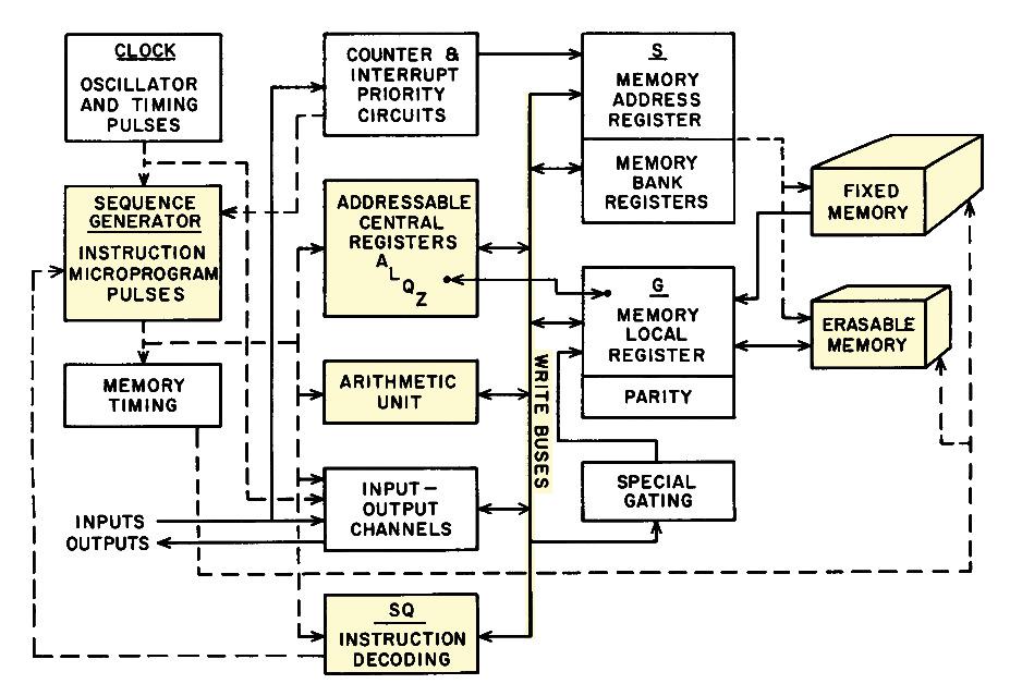
  1. The AGC had an internal bus, with multiple units writing to the bus which were electrically tied together.

    AGC architecture

  2. Some gates were saved by implementing the AGC's only bitwise instruction as a wired-OR:

    While most computers implement Boolean functions with logic circuitry in the ALU, the Apollo Guidance Computer manages to implement them without extra hardware. The OR operation is implemented through a trick of the register circuitry. By gating two registers onto the write bus at the same time, a 1 from either register will set the bus high, yielding the OR of the two values.

    source

    However, the AGC instruction set description shows that the only actual bitwise hardware instruction was MASK, which was a bitwise AND, instead of a bitwise OR. In any case, there were pseudoinstructions ("extracode") that implemented bitwise AND, OR, and XOR to the I/O ports: RAND, ROR, RXOR, WAND, and WOR.

\$\endgroup\$
-1
\$\begingroup\$

In addition to well-known truths about this configuration, I will add a few more considerations. They are accumulated through the years when I was thinking how to reveal the truth to my students so that they not only know what it is but understand why it is made so...

Open output

Output quantity. Actually, the output quantity of an open collector stage is resistance; it does not produce voltage or current. So, its output is passive, "dead"... and this device cannot supply a load... it needs an additional voltage source (the same or else's power supply in series to the load). In logic gates, this "resistance" is zero or infinite and the transistor is considered as a switch.

Wired OR

Logic function. The wired OR implements logic OR if we consider the input "0" as an active signal (TRUE). Actually, if we consider the input "1" as an active signal, this will be AND "gate" since the output will be high if both inputs are high. This trick is based on the De Morgan's laws and is used in diode logic gates where the AND logic gate is actually an OR gate.

Input flexibility. A great advantage of the wired OR "gate" is its flexibility - you can easily expand the number of inputs... and even vary it during the circuit operation without need of doing something more. A typical example of this configuration is the way interrupting sources are connected to the microcontroller IRQ input.

Perfect simplicity. I have put "gate" in quotes because it is actually just a node, point... i.e., nothing. Similarly, a "wired AND" is just a wire that we can cut at as many places as we want to include input "sources" (resistances, switches)... but this is not so convenient as the OR node. So, the OR "gate" consists of grounded switches (resistances) in parallel while the AND "gate" - of floating switches (resistances) in series.

Complementary output

The "problem" of the complementary output is that it can directly supply both ground and Vcc to the load which does not allow outputs to be joined. But still there are two situations when this connection does not lead to a conflict (short connection) between the outputs with opposite voltages:

1. Identical output signals. Although rare, it is possible to change the output signals in the same way, for example in order to increase the output current. Then the outputs help each other instead of "fighting".

2. "Forced" switching. Although it sounds unbelievable, it is possible for the outputs of two complementary stages to be connected even when they have different output voltages if two requirements are met:

  • the control output is more powerful than the controlled one
  • the controlled stage immediately changes its output voltage so it becomes equal to the control output voltage.

An example of such a "brutal" control is the write operation in an SPAM cell. You can see more about this trick in my RG question.

Complementary stage as open output

It is interesting to explain the role of OR-ing diodes connected in series to the complementary outputs with the purpose to make them "open outputs".

From another viewpoint, the "problem" of the complementary stage is that its output is bilateral: when the output voltage is high ("1"), it sources current to the load (if connected to ground); when the output voltage is low ("0), the output sinks current from the load (if connected to Vcc).

OR-ing diodes make the bilateral outputs unilateral. If the diode cathodes are connected to the outputs, they only sink a current from the load; if the diode anodes are connected to the outputs, they only source a current to the load.

You can see more about this explanation in my RG question.
\$\endgroup\$

Your Answer

By clicking “Post Your Answer”, you agree to our terms of service and acknowledge you have read our privacy policy.

Not the answer you're looking for? Browse other questions tagged or ask your own question.