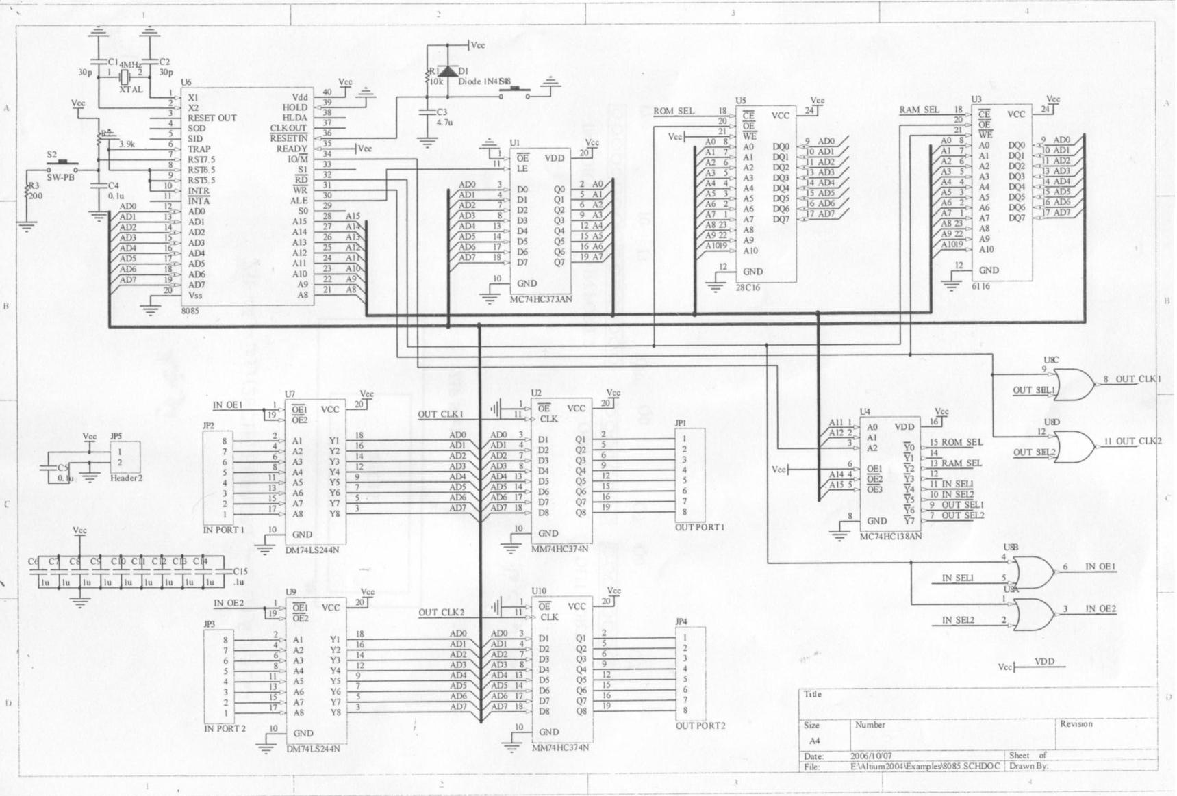
The above picture is an 8085-based system schematic used for undergrad courses at the laboratory. Now at first sight it seems that the 8085 in the circuit is isolated mapped IO since it uses the IO/M' signal, but when we are enabling IO/M' to write/read, the lines determining I/O ports are A11 and A12 (Where based on 8085 configurations we should only use AD0 to AD7 for determining I/O port). It is also not memory mapped because we are actively using the IO/M' signal.
My question is that is there something wrong with this circuit or if not how exactly is it operating and how can we write in the output ports?
Please consider that the synthesized circuit based on this schematic has been used in the laboratory. I am not completely sure if this exact design was used but it shouldn't differ that much.
\$\begingroup\$
\$\endgroup\$
3
-
\$\begingroup\$ It is using both I/O and Memory mapping. The 8085 uses the same multiplexed address lines for both memory and I/O. The IO/M selects one or the other, it is timed with the read and write signals. The ALE latches the upper address bits. If my memory is correct you can use as many address lines as you want, they will just roll over and repeat if not decoded. \$\endgroup\$– GilCommented May 14, 2021 at 2:31
-
\$\begingroup\$ @Gil: ALE latches the lower address bits. \$\endgroup\$– Dave TweedCommented May 18, 2021 at 12:30
-
\$\begingroup\$ Your are correct Dave, I was tired and goofed. I have not used that part since about 1985. \$\endgroup\$– GilCommented May 20, 2021 at 2:59
Add a comment
|
1 Answer
\$\begingroup\$
\$\endgroup\$
It's I/O mapped. That's really the only thing it could be, with IO/M driving A2 of the decoder.
The piece of information you're missing is that
When 8085 executes IN or OUT instruction, it places device address (port number) on the demultiplexed low order address bus as well as the high order address bus.
from here.
So, this is a perfectly legitimate way to decode I/O addresses.

