0
\$\begingroup\$

I have designed a simple PCB with the follow layers

  1. Top Layer, high speed traces (rest ground copper)
  2. Inner 1, Ground Copper area everywhere apart on the very left side where the trace antenna will be places and appart from the vias between bottom and top, however no traces on this layer
  3. Inner 2, Power lines only (5V, 3.3V, 4V)
  4. Bottom Layer, some low speed traces and some vias for the high speed traces go on bottom layer in order to facilitate their tracing. (rest ground copper)

The trace antennas I see are usually top and bottom layer but since the antenna is high speed, shall I only use the traces of it only on the top layer? On the following picture you can see the antenna, Red is the Top and Blue the bottom layer. Can I leave it like this or I should turn everything red?

Are there any comments/recommendations for the layering that I did(high speed top, low speed bottom and few vias for the high speeds on bottom aswel?

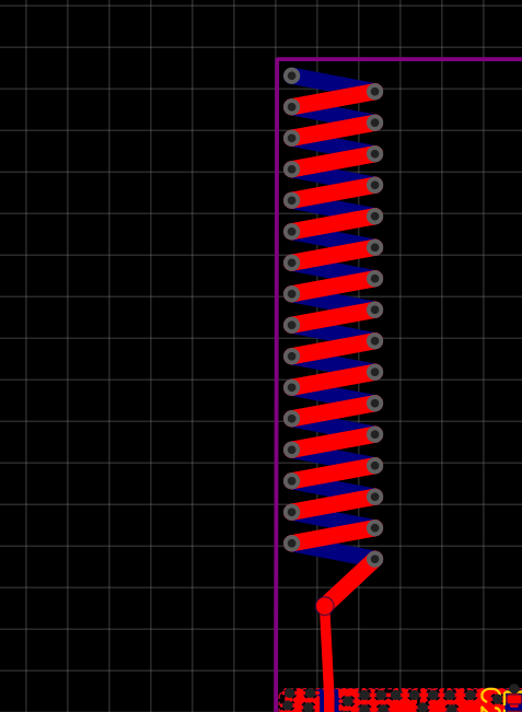
enter image description here

\$\endgroup\$
3
  • \$\begingroup\$ I believe the general recommendation is to avoid vias entirely when dealing with 50 ohm impedance-matched signals and keep everything on a single layer. But then I'm not a RF designer so don't take my word for it. \$\endgroup\$
    – Lundin
    Commented May 28, 2021 at 10:34
  • \$\begingroup\$ if all components are on top layer but they have to be routed as low speed signals on bottom layer, how can they be avoided? i am not too experienced with designing if you could please help me ( i heared high speed signals top layer,low speed bottom layer) \$\endgroup\$
    – Kris
    Commented May 28, 2021 at 10:52
  • \$\begingroup\$ @Lundin - Vias can be used with RF, but they have to be designed properly, and not just dropped in blindly (pun intended) through a hole in the substrate. We routinely use them at frequencies over the entire RF gamut, from 400 MHz to over 50 GHz. \$\endgroup\$
    – SteveSh
    Commented May 29, 2021 at 19:11

2 Answers 2

2
\$\begingroup\$

Pay attention to the dimensions of the antenna elements. You should copy the reference design exactly, and not modify it. The antenna traces should be at the external layers, Top and bottom.

\$\endgroup\$
2
\$\begingroup\$

I wouldn't deviate from the reference design, at all. If that antenna doesn't suit your needs, you should find a difference reference design :)

For example, this antenna is a flattened approximation of a helical (coiled spiral) design. So, it's not just the length of the antenna, but also the depth of the pcb substrate, which is critical to the design. The reference design probably mentions a pcb thickness. You want to make sure to match it.

As far as which layers, it is usually the outer layers (top and bottom). But, again, this depends on the reference design.

\$\endgroup\$
1
  • \$\begingroup\$ Can't emphasize enough bitsmack's recommendation to don't deviate from the reference design. Unless you are well versed in RF/microwave design and know how use field solvers and other RF analysis tools, you're probably just going to make things worse by making arbitrary changes, \$\endgroup\$
    – SteveSh
    Commented May 29, 2021 at 16:53

Your Answer

By clicking “Post Your Answer”, you agree to our terms of service and acknowledge you have read our privacy policy.

Not the answer you're looking for? Browse other questions tagged or ask your own question.