2
\$\begingroup\$

I'm designing a 4-layer PCB, containing a GPS module (u-blox NEO M9N) and a Taoglas antenna. The GPS antenna should be on the top layer, and the GPS receiver should be on the bottom layer.

Besides the GPS module, my board will have other components like a microcontroller and a CAN transiever.

Due to u-blox recommendations, one of the layers will be specifically intended for the ground plane.

The other internal layer will be used for communication signals (CAN and UART) and for supplying the ICs (all ICs are low power). The signals will start from their respective ICs and pass through the internal layer using a via(drill, hole). I did this so that there would be no communication signals in the GPS and antenna layers. I want these layers to have only tracks related to GPS signal reception.

What do you think of my design decisions? Are there problems carrying signals in an inner layer? u-blox recommends not passing signal trails near the GPS receiver.

Thank you so much

Layers: 1 (external) - Antenna;

2 (internal ) - Ground Plane;

3 (internal) - Signals;

4 (external) - GPS MOdule.

Thanks for the answers. The board was designed and will be manufactured. The tips helped to have a good project.

\$\endgroup\$
1
  • \$\begingroup\$ Please see the edit \$\endgroup\$
    – Voltage Spike
    Commented Jun 7, 2021 at 21:45

2 Answers 2

3
\$\begingroup\$

The GPS antenna should be on the top layer, and the GPS receiver should be on the bottom layer.

If you can, get a through hole component for the antenna connector (either that or keep it on the same side of the board), this will allow you to keep the trace running from the antenna connector to the Ublox a continuous transmission line (the M9N needs 50Ω) from connector (switching layers with a matched transmission can be difficult as you have to match the vias, and can also incur a small loss). Make sure the trace is a 50Ω transmission line and the shorter the distance between M9N and antenna connector the better.

Also for most transmission lines (micro strip line), the ground plane needs to be directly under the microstrip line. Here is a calculator: https://www.eeweb.com/tools/microstrip/

Also it doesn't matter as much if the signals get close to the M9N because they do anyway on the inside of the module. You can see an example of this here: https://www.sparkfun.com/products/15733 and this product works well.

On the modules that I've designed and would be the recommended stackup.

Layers: 1 (external) - GPS MOdule\Antenna\signals;

2 (internal ) - Ground Plane;

3 (internal) - Power;

4 (external) - More signals.

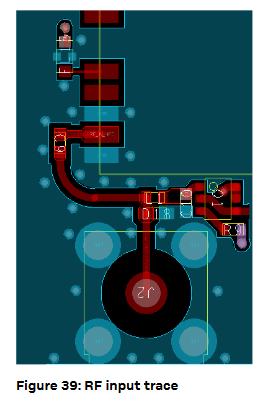
Also the manual recommends keeping the RF_IN trace on the top layer with a continuous ground plane underneath:

enter image description here
Source: https://www.u-blox.com/en/docs/UBX-19014286 pg82

The RF_IN trace on the top layer should be referenced to a suitable ground layer.

\$\endgroup\$
0
1
\$\begingroup\$

What you suggest is ok, but I’m not sure why you feel the need to dedicate an entire layer to the GPS signals. You’ll want to keep the GPS antenna as short as possible and have a little clearance from other signals but there’s no more of a problem having signals on the same layer than having them on an adjacent layer. But if you want to lay your board out the way you suggest then that’s up to you, the only downside might be that vias introduce a small inductance and so for high-speed signals you would want to have as few as possible.

\$\endgroup\$

Your Answer

By clicking “Post Your Answer”, you agree to our terms of service and acknowledge you have read our privacy policy.

Not the answer you're looking for? Browse other questions tagged or ask your own question.