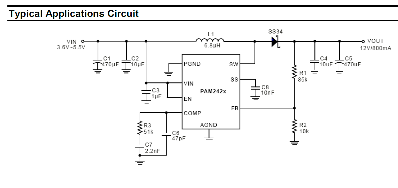
I'm trying to a boost conveter PAM2423 which workd at 520kHz for the first time(using a high quality breadboard from jameco for prototyping) following the manufacturer ref schematic:
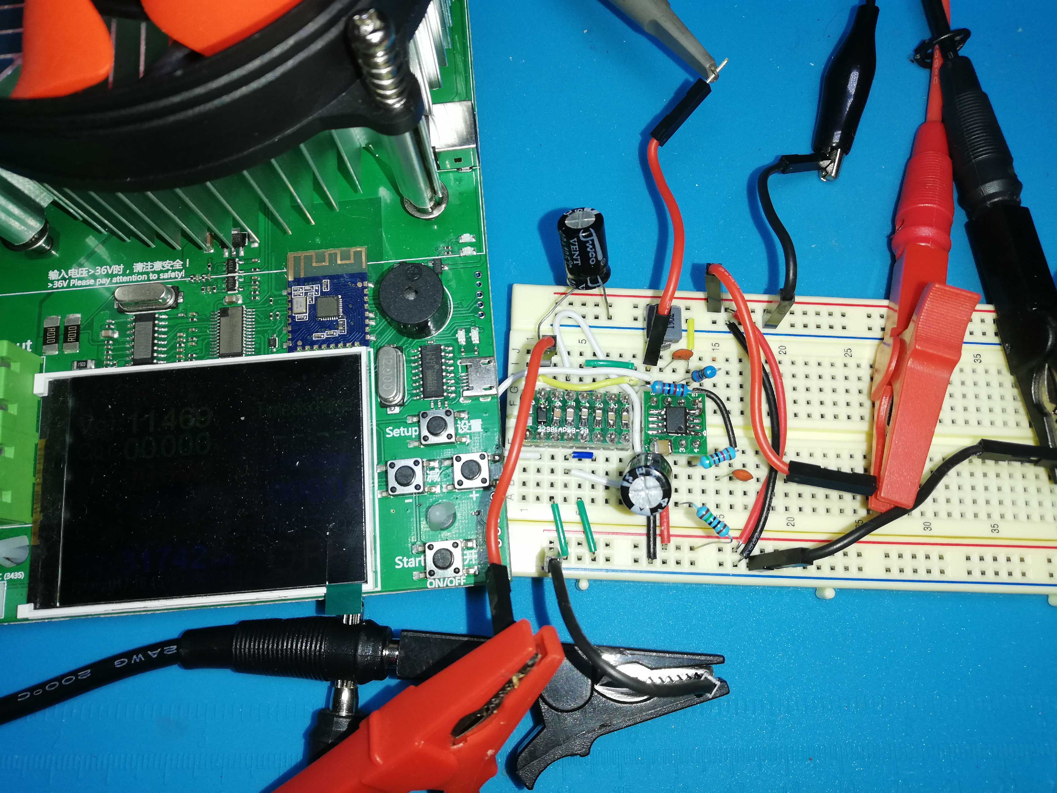
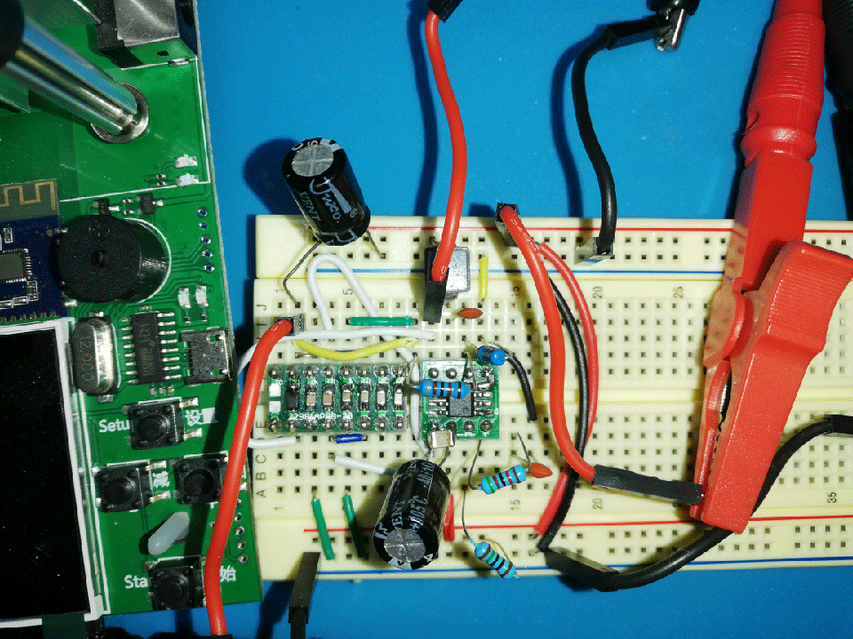
My Setup:
I've soldered a 10uF input ceramic capacitor directlly to the chip
and unlike the manufacturer schematic I've added a 150OHM resistor between the VIN and EN pin because I've suspected shorting it directly burned the last IC. I'm using the PA4341.682NLT 6.8uH 4.5A as the inductor if that matters(of course connected as closely as possible to the IC's output)
The PGND and AGND along with the button pad are connected to the same GND.
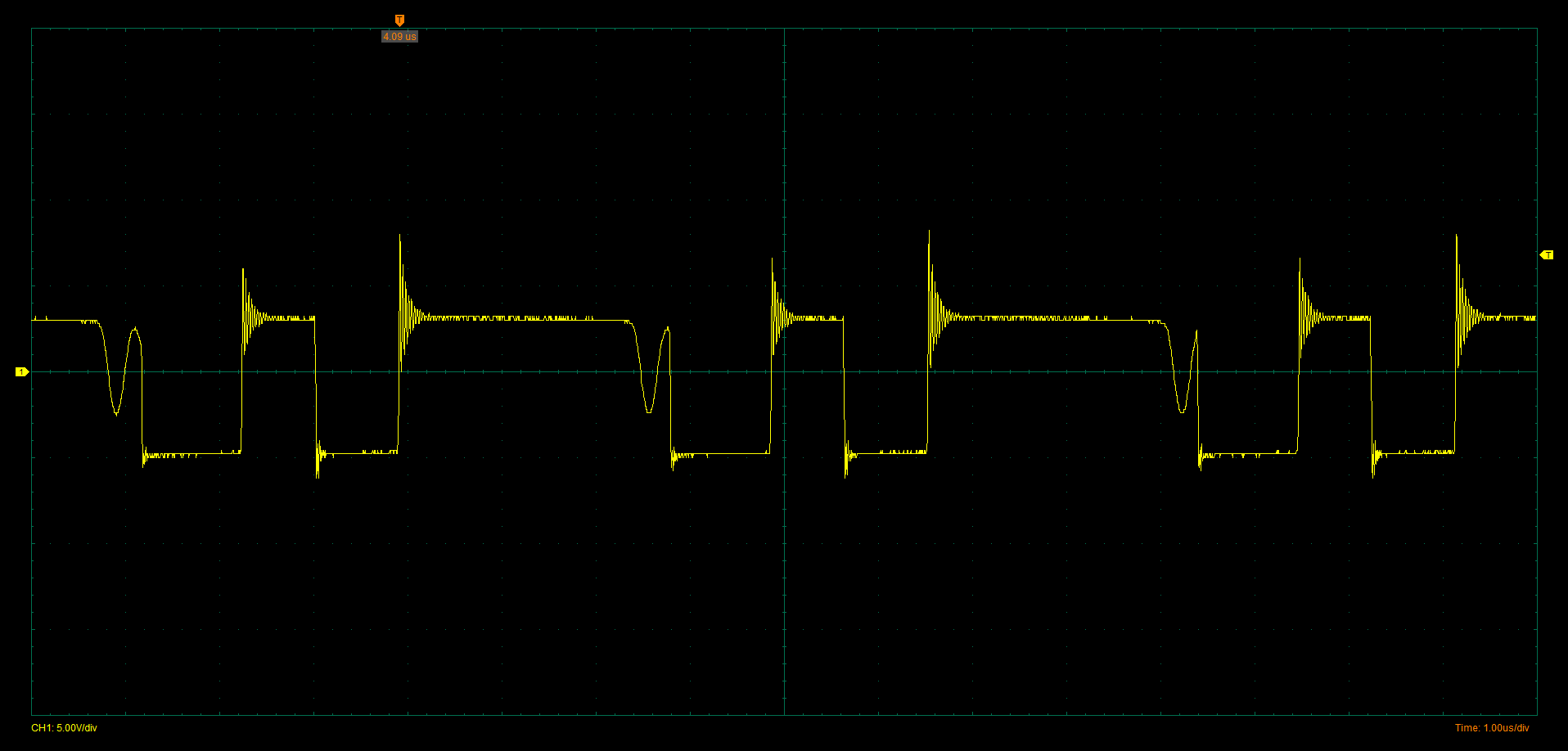
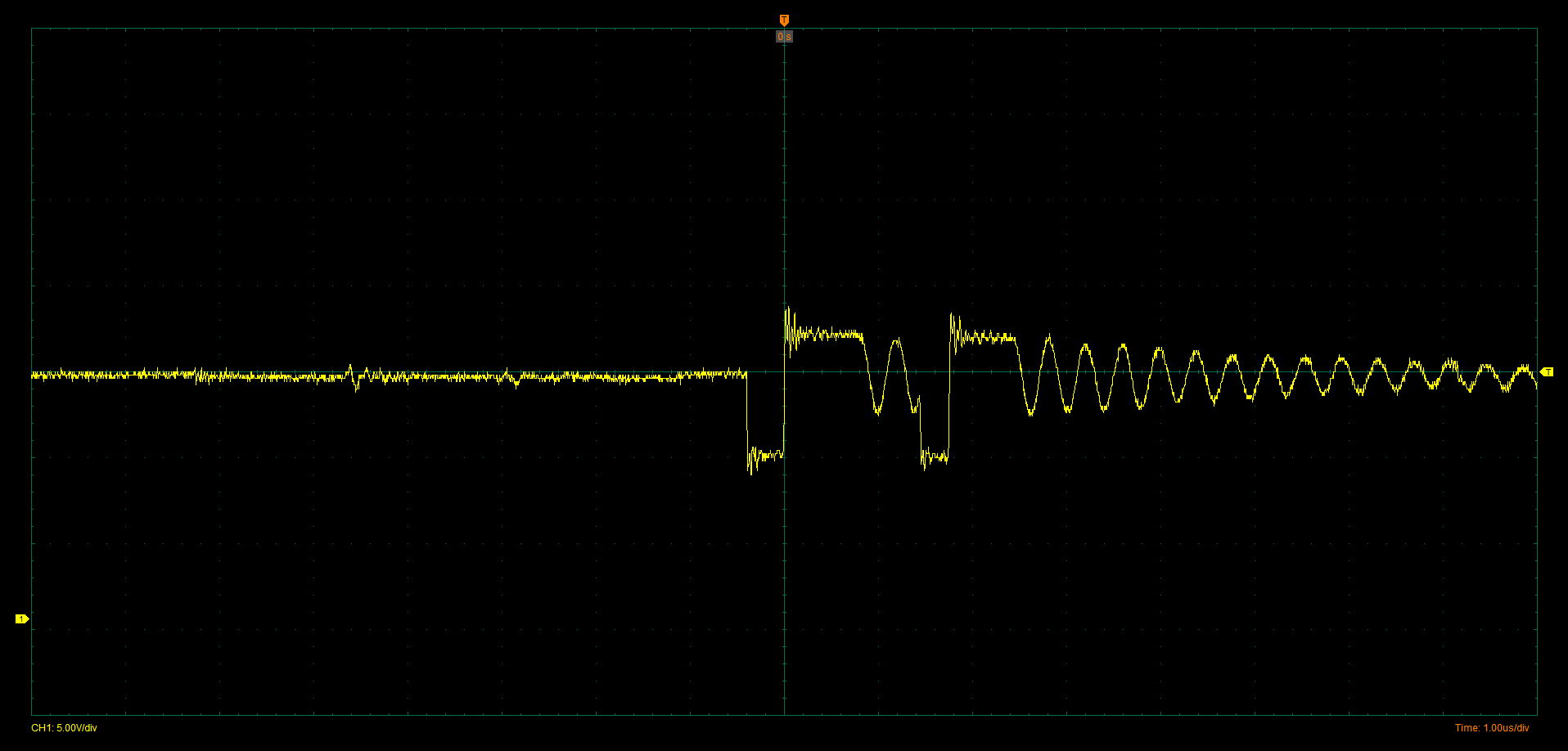
Here is the scope output connected between SW Pin of the IC and GND connected to an E-load @ CC 0.1A with VIn = 4.2V and Average (not that stable) output voltage of 6.5V:
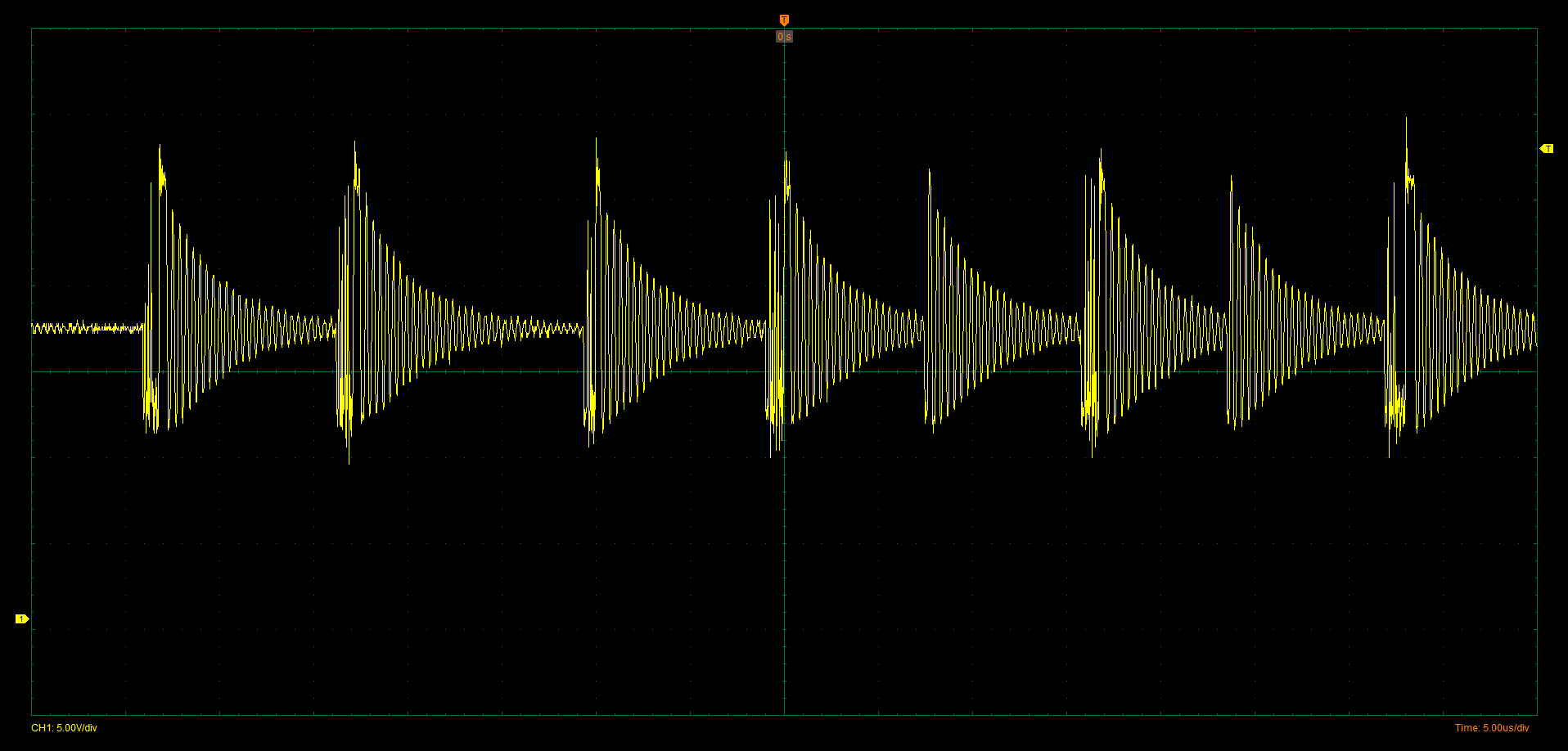
and @ No load VOut = 11.1V the SW output looks like this:
I'm not realy sure how to tune the COMP pin sins there is not alot of info in the datasheet about it(other than voltage setting no guide equations) but increasing C7 and decreasing R3 seem to make things a little better.
What could be wrong about the design? What exactly does that Compensation pin translates to? Could the values in the schematic be wrong?

