5
\$\begingroup\$

I'm working on designing a buck converter, and I've been using LTspice to simulate the circuits. However, it seems that I'm misunderstanding something.

My understanding is that one should not use an N-channel MOSFET for high-side switching, but when I was researching buck converter design, I came across two separate videos that used schematics with high-side N-channel MOSFETs. Below are the links to these videos with embedded time stamps to the schematics I'm referencing (no need to watch the entire videos):

https://youtu.be/uI7OWTCDc6M?t=10

https://youtu.be/IpoI6ERn5zM?t=240

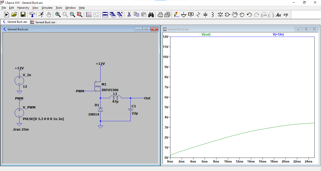
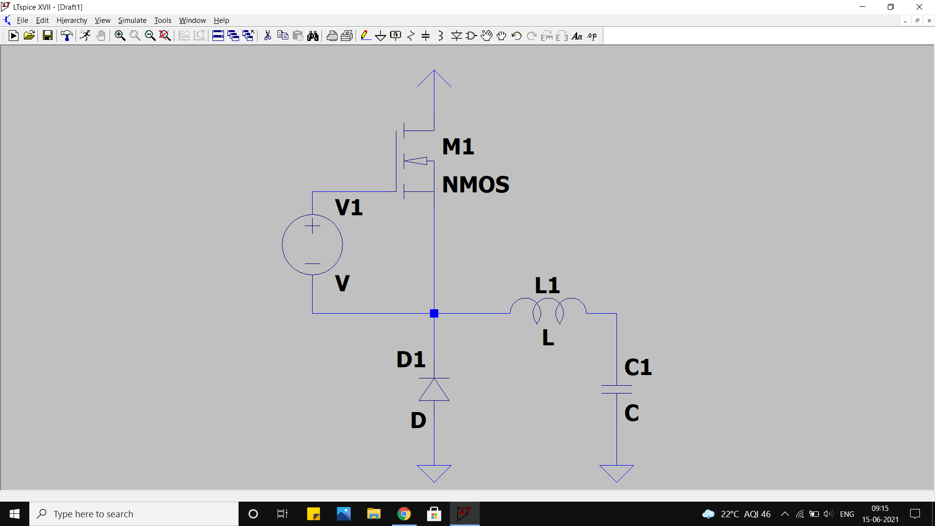
I wasn't convinced that this should work, so I whipped up a schematic in LTspice to model this. But lo and behold, it seems that an NMOS on the high side is indeed resulting in buck conversion.

Buck converter with an NMOS

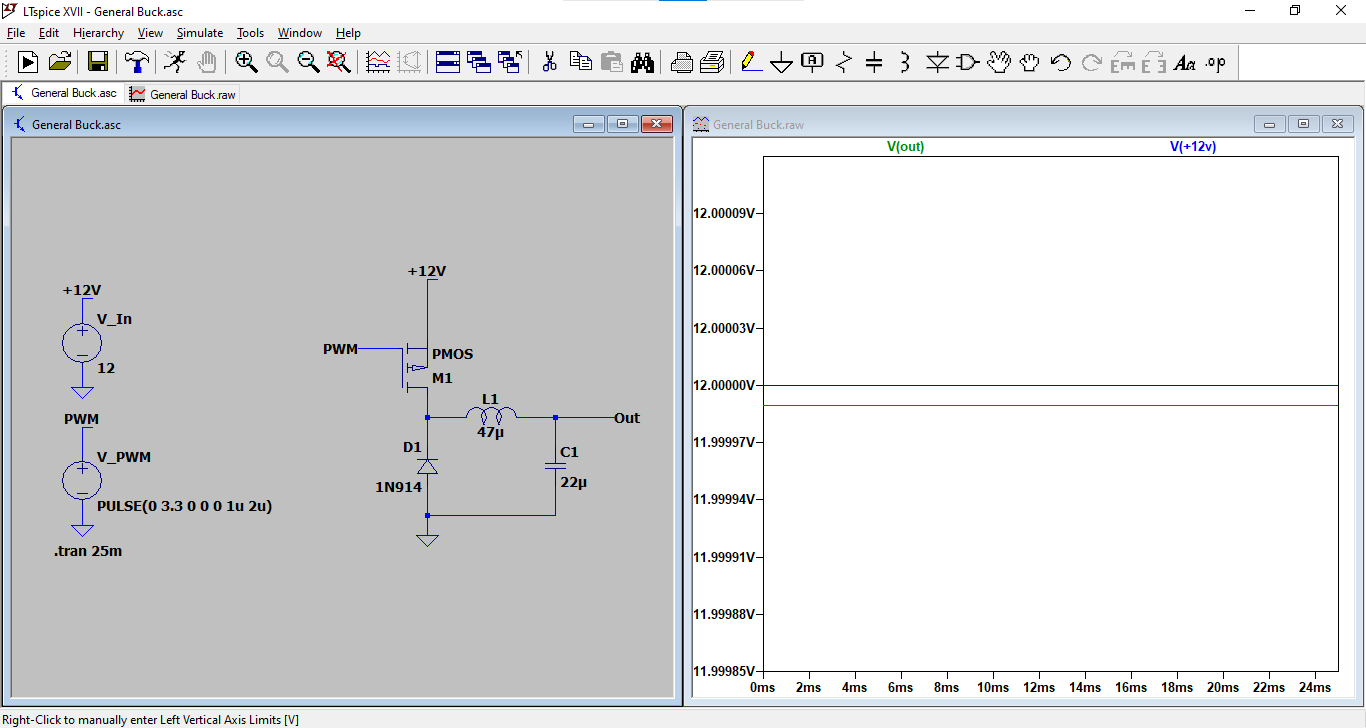
What's more, when I replaced the NMOS with a PMOS, the voltage wasn't bucking at all.

Non-buck converter with a PMOS

I feel like I'm losing my marbles. What's going on here?

\$\endgroup\$
2
  • 1
    \$\begingroup\$ The linked tutorials are probably correct (not gonna watch youtube videos) : you certainly can use NMOS on the high side switch, but you need to learn the correct gate drive technique for NMOS as a high side switch. 0 to 3V ain't it. \$\endgroup\$
    – user16324
    Commented Jun 14, 2021 at 21:31
  • \$\begingroup\$ Sorry, I didn't intend for users to watch them, but rather open them up just to see the schematics (the time stamps are embedded in the link). I'll edit the question to make that more clear. \$\endgroup\$ Commented Jun 14, 2021 at 23:04

6 Answers 6

7
\$\begingroup\$

NMOS devices require a positive Vgs to turn on - that means the gate voltage must be higher than the source voltage.

In your circuit you are driving the gate with a 0-3.3V signal, which means the source voltage, and hence output voltage, can never be more than 3.3V (less the threshold voltage to have any significant current flow), otherwise the MOSFET turns off again.

To do high-side switching with an NMOS device, you need a floating gate drive circuit - your 0-3.3V signal needs to be shifted to track the source node rather than ground. This is typically accomplished using a floating power supply (bootstrap circuit, or isolated DC/DC), in combination with a signal isolator (opto-coupler, digital isolator, etc.).

\$\endgroup\$
1
  • \$\begingroup\$ Okie dokie, so am I understanding you correctly if I now conclude that the first schematic is not demonstrating buck conversion, but rather the limitations of the NMOS? And would I be correct to say that the linked tutorials got it wrong? \$\endgroup\$ Commented Jun 14, 2021 at 21:04
4
\$\begingroup\$

You are driving your FETs (both of them!) improperly. The \$\mathrm{V_{GS}}\$ must meet or exceed the amount specified for the FET's rated \$\mathrm{R_{DSON}}\$.

Note that it's your responsibility to make sure that \$\mathrm{V_{GS}}\$ does not exceed its rated maximum in either direction.

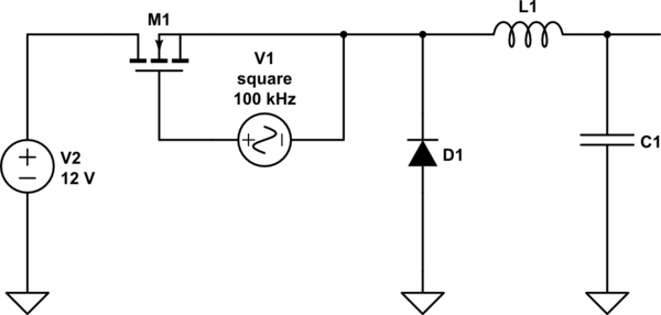
For the NMOS case, drive \$\mathrm{V_{GS}}\$ from \$0\mathrm V\$ to \$+12\mathrm V\$ (or \$+5\mathrm V\$ if you have a logic-level FET). This will require a gate driver or other circuit "magic".

schematic

simulate this circuit – Schematic created using CircuitLab

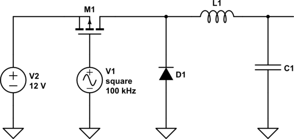
For the PMOS case, drive \$\mathrm{V_{GS}}\$ from \$0\mathrm V\$ to \$-12\mathrm V\$ (yes, minus -- or \$-5\mathrm V\$ if you have a logic-level FET). For the right input voltage, you just need to drive \$\mathrm{V_{G}}\$ from supply to ground -- which is kinda what's pictured here.

schematic

simulate this circuit

\$\endgroup\$
6
  • \$\begingroup\$ Hey! Thanks for the answer and the schematics; these are helpful! I am a little bit hazy, though, on the difference between your PMOS schematic and mine. Unless I'm just sleep-deprived (which is very possible), it looks to me like the gate drive in both schematics go between the gate and ground with no further connections. (Specifically, I'm understanding a gate drive between the input and the gate implying that there should be some sort of connection to V2, presumably through a resistor. Am I misunderstanding?) \$\endgroup\$ Commented Jun 15, 2021 at 1:59
  • 1
    \$\begingroup\$ Edited for clarity. In the PMOS case, you were driving from \$0\mathrm V\$ to \$3.3 \mathrm V\$. This meant that the FET never got turned off. You needed to drive it from the supply voltage (\$\mathrm{V_{GS}} = 0\$) to turn it off, and to ground (\$\mathrm{V_{GS}} = -12\mathrm V\$) to turn it on hard. \$\endgroup\$
    – TimWescott
    Commented Jun 15, 2021 at 3:52
  • \$\begingroup\$ @FluffytheTogekiss Another thing worth mentioning is you goofed up your original PMOS LTspice schematic by not choosing an actual part number. The default PMOS SPICE model uses a Vto (zero bias threshold voltage) of 0V. That's going to cause tons of screwiness. \$\endgroup\$
    – Ste Kulov
    Commented Jun 15, 2021 at 6:50
  • \$\begingroup\$ @TimWescott Ah, I see! Thanks! \$\endgroup\$ Commented Jun 15, 2021 at 14:13
  • \$\begingroup\$ @SteKulov Oof, rookie mistake. >.< Thanks for pointing that out! \$\endgroup\$ Commented Jun 15, 2021 at 14:13
4
\$\begingroup\$

The high-side NMOS gate requires a control voltage that's higher than the drain by at least one gate-source threshold. With only a 3.3V gate-source voltage (Vgs) driving it your FET will never turn on fully: the switching node will go only as high as 3.3V - FET threshold. This will limit the output to about 2V, where you should be getting about 6V. Worse than that, the FET will be dissipating a lot of power.

With the PMOS, you have the opposite problem: your FET is never turning off, because the gate voltage never gets close enough to the source to do so.

The quick fix for your sim is to make the pulse generator output 12V for PMOS, and 15.3V or more for NMOS.

You can also do the following:

  • NMOS: tie pulse gen (-) to source, that is, the switching node
  • PMOS: tie the pulse gen (+) to source, that is, Vin.

The point is, for both cases, some hind of higher-than-logic voltage gate driver is needed. Additionally, for NMOS that gate drive (Vgs) must be higher than the Vin supply by at least one gate-source threshold; preferably even more than that to minimize on resistance Rds(on) and reduce losses. How to do that? Read on.


In an actual device using NMOS high-side FETs there's a trick to dealing with this issue: use a bootstrap voltage generator to make the high-side gate driver supply.

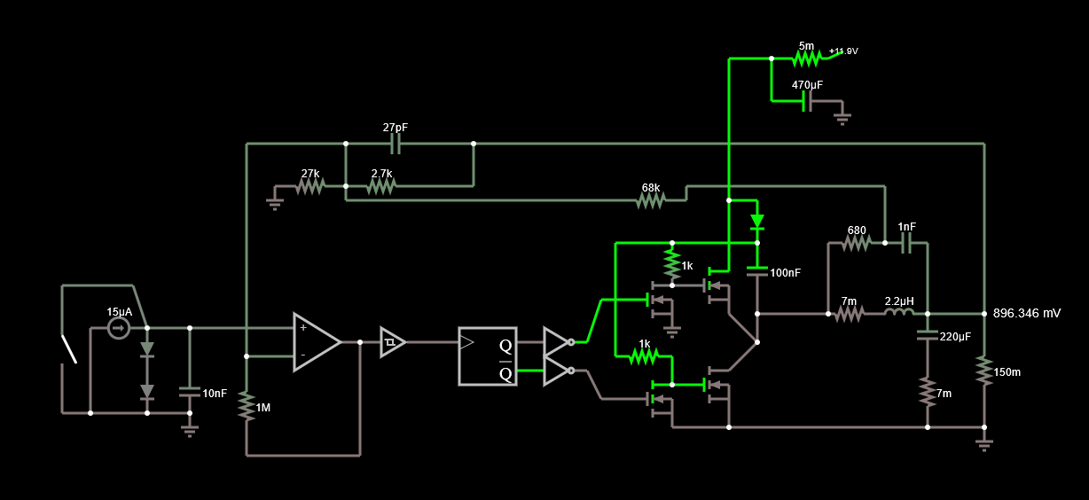
Below is a Falstad sim of a constant-on-time synchronous buck that uses boostrap high-side drive (Try it here).

enter image description here

The boostrap is generated by the cap from the switch node to the diode, which is forward biased when the high side turns on. This voltage swings from Vin to 2*Vin, which gives plenty of drive to the high-side NMOS well into its low-resistance range.

\$\endgroup\$
3
  • 1
    \$\begingroup\$ "higher than the drain by at least one gate-source (Vgs) threshold" maybe in theory. In reality you want ot be higher than the drain by the \$\mathrm{V_{GS}}\$ at which the FET's \$\mathrm{R_{DS ON}}\$ is specified. That's usually 12V for a "regular old" FET, and 5V or 3.3V for a "logic-level" FET. \$\endgroup\$
    – TimWescott
    Commented Jun 14, 2021 at 22:07
  • 1
    \$\begingroup\$ Yes, that’s quite true. In the context of the Q though the larger point is understanding the need for the lifted gate drive, and a typical way to achieve that. Rds(on) vs. Vgs is an additional improvement opportunity once they have their sim working at all. \$\endgroup\$ Commented Jun 14, 2021 at 23:54
  • \$\begingroup\$ Ooh, I remember getting a surface-level introduction to bootstrapping a while back, but the schematic I saw wasn't intended for high-frequency switching. This should be very helpful for learning about more robust implementations. Thanks for this! \$\endgroup\$ Commented Jun 15, 2021 at 2:00
2
\$\begingroup\$

In the 1st video the gate got V2=+24V pulses. The mosfet was working as cathode follower. The pulse output to the coil was V2 minus gate treshold voltage. That means +21V pulses to the joint of the diode and coil.

When the mosfet was ON there were massive 3V voltage drop as Vds. That would cause unacceptable losses when compared to what's generally possible with buck regulators.

Some kind of bootstrapping or feeding Vgs pulses through transformer directly between g and s is needed for proper operation. The gate pulse voltage of the high side N-mosfet should rise to 27...30V to let the output from the source be as near the +24V input as possible.

The video presented only the core idea of buck switching, it was not an example of good design.

If there's no load but pulses are switched regularly, the output voltage can rise slowly to the gate input voltage as your own example shows. But that's NOT buck regulating operation, it should be considered more as leakage.

Your P-mosfet example is non-working. The mosfet is ON all the time because Vgs is never 0.

BTW. These circuits skip totally the voltage regulation operation which needs a feedback controller.

\$\endgroup\$
4
  • \$\begingroup\$ This is very helpful. Thanks! Quick follow-up: On the PMOS variant, I originally had a pullup resistor to +12V to try to get Vgs to 0, but since the PWM signal sets the voltage instead of opening the circuit, this didn't work. I think I could open the circuit with a logic-level signal by using another NMOS at the gate, but in your experience, is there a way to do this without introducing a second transistor? \$\endgroup\$ Commented Jun 15, 2021 at 1:50
  • 1
    \$\begingroup\$ In practical circuits some transistor must feed the gate voltage to the high side P-channel mosfet. That transistor can be a part of the voltage controlling circuit. It pulls the gate towards GND for ON state. A working buck switcher with real voltage regulation ability can be made with as few as 3 transistors including the high side switch, no IC's are needed. Of course, IC controllers can have all kinds of security measures and contain also the switch for low power applications, so they are the practical way to make perfect designs. \$\endgroup\$
    – user136077
    Commented Jun 15, 2021 at 6:32
  • 1
    \$\begingroup\$ @FluffytheTogekiss (continued) If you plan to use PWM signal from a computer the 2nd transistor is the simplest way to drive the high side gate. Pulse outputs of the computers very likely cannot stand high enough voltage. I guess that's your problem. Otherwise you would only insert a diode. A transformer or opto coupler could also be used, but transformer needs careful design and fast enough OC also is tricky. \$\endgroup\$
    – user136077
    Commented Jun 15, 2021 at 7:13
  • \$\begingroup\$ I see. Thanks so much for your answer and insights! \$\endgroup\$ Commented Jun 15, 2021 at 14:34
1
\$\begingroup\$

when I replaced the NMOS with a PMOS, the voltage wasn't bucking at all.

Because you are using a 3.3V PWM, the P-Channel MOSFET never turns off. Because of this, your output voltage is equal to the input voltage.

Why does the PFET never turn off? Its because the Vgs of the PMOS when the PWM signal voltage is 3.3V is (12-3.3V) = 9V (approx), which is high enough to keep it on. When the PWM voltage is 0V, the PMOS will obviously be on. You need a PWM voltage of 12V to properly turn of the PMOS.

I wasn't convinced that this should work, so I whipped up a schematic in LTSpice to model this. But lo and behold, it seems that an NMOS on the high side is indeed resulting in buck conversion.

Although it may seem that the buck converter is running properly, its not. This is because the N-Channel MOSFET is not driven correctly and is running hot as it is actually conducting in its saturation mode. You can press ALT+ENTER after dragging your curser over the NMOS in your simulation to see the power dissipation.

In order to drive your NMOS properly, you need to re-configure the square wave generator like so:

enter image description here

and increase the PWM voltage to at least 5V in case of a logic level MOSFET or 10V in case of a "normal" MOSFET.

\$\endgroup\$
0
\$\begingroup\$

The NMOS FET circuit is your 1st circuit simulation. So, you provide the drive signal to the NMOS FET: VinputPWM.
Provide a load resistor: call it Rload or Rout: it is the circuit that you power with this buck-converter circuit.
Let Rout = Rload draw 0.5 amps; then Rload = 24 ohms. 12V / 24 ohms = ~ 0.5 amps V = IR: 12Volts = [ (I= 0.5amps) * (Rds + Rind + Rout)] .
Let Rds = 0.2 ohms, and Rind = 0.1 ohms, and Rout = 24 ohms.

The NMOS FET needs a VinputPWM. “drive signal”.
The FET has a datasheet value: Vgs minimum is ~ 10V. The PWM signal swings from Vpwm = 0vdc to +10Vdc. When Vpwm = 10V, the FET is on hard, and there is very little voltage drop across M1drain and M1source. The FET is off when Vpwm = 0; A pulse-width modulated waveform is applied to the load that sustains a steady output voltage and ( draws a steady 0.5 amps ), that will be provided to the CiRCUIT (called Rload). The output current is provided to the load: directly thru the FET, and then thru the diode D1, taking turns.

The PMOS FET circuit is your 2nd circuit simulation. So, you provide the drive signal to the PMOS FET: VinputPWM.
Provide a load resistor: call it Rload or Rout: it is the circuit that you power with this buck-converter circuit.
Let Rout = Rload draw 0.5 amps; then Rload = 24 ohms. 12V / 24 ohms = ~ 0.5 amps V = IR: 12Volts = [ (I= 0.5amps) * (Rds + Rind + Rout)] .
Let Rds = 0.2 ohms, and Rind = 0.1 ohms, and Rout = 24 ohms.

The PMOS FET needs a VinputPWM. “drive signal”.
The FET has a datasheet value: Vgs minimum is ~ -10V. The PWM signal swings from Vpwm = 15vdc to +5Vdc. When Vpwm = 5V, the FET is on hard, and there is very little voltage drop across M1drain and M1source. The FET is off when Vpwm = 15; A pulse-width modulated waveform is applied to the load that sustains a steady output voltage and ( draws a steady 0.5 amps ), that will be provided to the CiRCUIT (called Rload). The output current is provided to the load: directly thru the FET, and then thru the diode D1, taking turns.

\$\endgroup\$

Your Answer

By clicking “Post Your Answer”, you agree to our terms of service and acknowledge you have read our privacy policy.

Not the answer you're looking for? Browse other questions tagged or ask your own question.