1
\$\begingroup\$

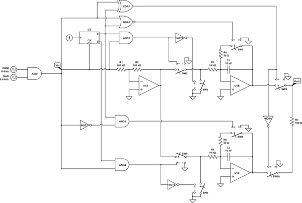
For theory-learning purposes I wanted to see if I could design a DAC that converts a 10 kHz PWM duty cycle to an analog waveform in a sample-and-hold manner with leap-frogging capacitive integrators, so that the charge-discharge ripple seen in a simple RC DAC is not present. My first stab at it uses ideal switching to focus on the basics:

schematic

simulate this circuit – Schematic created using CircuitLab

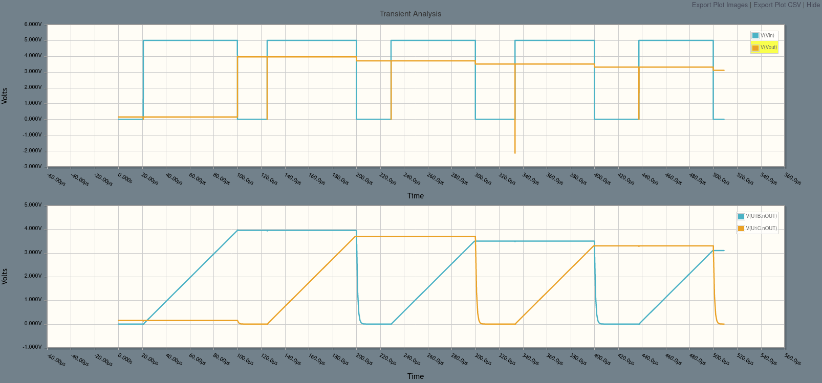
For each integrator, there are basically four segments: discharge, charge, output, output. This more or less works:

transient

The two PWM inputs are to simulate a single input whose duty cycle is changing.

Problems I see:

  • There are some glitches around the logic transitions
  • Any mismatch in the time constants between the two integrators is going to create square ripple cycle to cycle
  • This seems more complicated than it needs to be
  • I needed R7 because one of the glitches looks like temporary contention between the two integrator outputs
  • In its current configuration, the integrators require the inverter of U1A, which in turn would require a negative voltage supply I'd prefer not to need
  • Though this should reduce ripple when compared to a simple RC DAC, the square transitions from level to level will create aliasing components in the spectrum at multiples of the PWM frequency, and these components might themselves require an antialiasing RC stage anyway to get rid of

Questions:

  • Is this at all a standard approach to DAC design? If so, what's it called?
  • If implemented correctly, what advantages and disadvantages are there to this approach when compared to simple RC other than complexity?
  • For the switches, would single MOSFET pass-gates suffice?
  • How can this be simplified?
  • How best to reduce the glitches?
  • Can R7 be dropped?
\$\endgroup\$
9
  • \$\begingroup\$ What are your specs? Ripple. Aliasing. Transient duration & amplitude . Impedance. Sampling rate. Never seen anything like this but here are many other types of multi-phase DAC’s google.ca/search?q=multi+phase+dac&ie=UTF-8&oe=UTF-8 \$\endgroup\$
    – D.A.S.
    Commented Jun 27, 2021 at 16:38
  • \$\begingroup\$ It seems to me that you might be wasting your time with this approach because, whatever trick you may employ, there are errors generated when the logic power rails change in voltage i.e. the integrators ramp quicker or slower. OK I may be wrong about this and you may have a cunning circuit that overcomes this basic problem. If I'm right, then you might just as well use an analogue filter of high order to recover the analogue signal from the PWM. If I'm wrong then apologies. \$\endgroup\$
    – Andy aka
    Commented Jun 27, 2021 at 17:06
  • \$\begingroup\$ @Andyaka For the charge rate to be affected, the logic level of the input itself would have to have an error, or maybe a pass gate would have to present a nontrivial voltage drop on SW2. Is that what you mean? \$\endgroup\$
    – Reinderien
    Commented Jun 27, 2021 at 17:25
  • 1
    \$\begingroup\$ The clocks will have to be impeccable otherwise summing will not give the "smooth" staircase voltage you seek -- it will have gaps and spikes. The switches will not help, either. This is close to the problems switched capacitor filters have. You might correct it with some filters, but then you're back at what you're trying to avoid. I've seen this in frequency detectors: filter signal, bandpass/matched/locked-in/etc filter, convert to pulse, integrate, sample&hold, calculate, but digitally (except initial filtering). \$\endgroup\$ Commented Jun 27, 2021 at 19:44
  • 1
    \$\begingroup\$ I'd be inclined to implement a filter with zeroes at the PWM frequency. \$\endgroup\$
    – Neil_UK
    Commented Jun 27, 2021 at 20:06

2 Answers 2

1
\$\begingroup\$

Is this at all a standard approach to DAC design? If so, what's it called?

It does not seem to be a standard approach. I only found a few examples of 'proposed' circuits that use a similar technique, including this one which describes itself as a 'synchronous PWM-DAC filter' (beware: not tested!):-
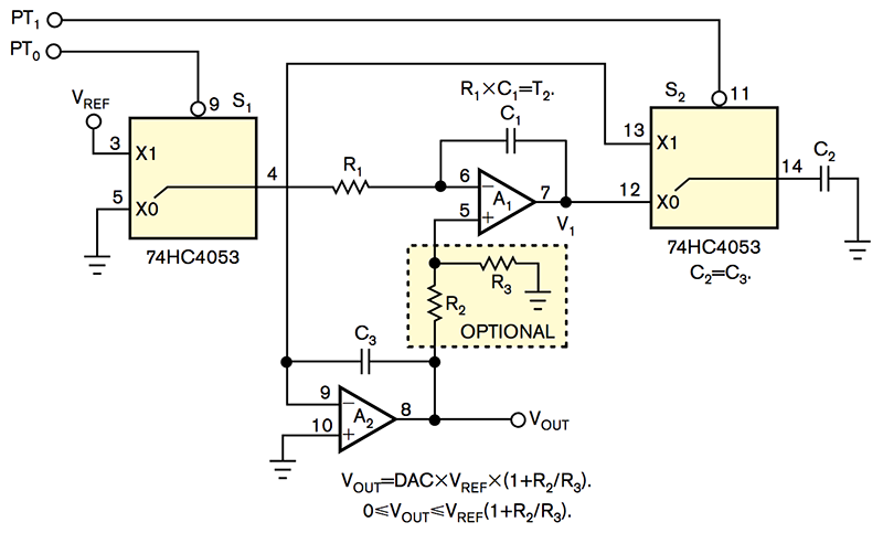
enter image description here

If implemented correctly, what advantages and disadvantages are there to this approach when compared to simple RC other than complexity?

The obvious advantages are much faster settling time without the need for a complex filter, and probably much shorter delay.

Disadvantages include (as you mentioned) possible mismatch between the two halves, greater chance of introducing distortion and glitches, and an inability to handle close to 0% and 100% PWM. Another limitation is that output voltage is proportional to PWM 'on' time - not the ratio of 'off' to 'on' - so it will not adjust itself to the PWM period.

For the switches, would single MOSFET pass-gates suffice?

Yes, provided they can be biased properly and reverse voltage drop is low when 'open'. I think this is doable for all but the output switches (for which a 'bidirectional' analog switch such as the CD4053 might be needed).

How can this be simplified?

I used a slightly different approach with a switched current source alternately charging two 'ramp' capacitors, which are then alternately connected to a single sample-and-hold capacitor. By making the s&h capacitor small compared to the ramp capacitors I was able to eliminate buffer amps between them, and the single current source means balance is assured if the ramp capacitors have equal values. The four PWM phases are arranged so that the processes of charge, hold, and discharge are separated enough to avoid interaction - at least for PWM ratios not too close to 0% and 100%.

Here's the LTspice simulation (the current source and switches are 'ideal' simply because I couldn't be bothered putting in 'real' components):- enter image description here
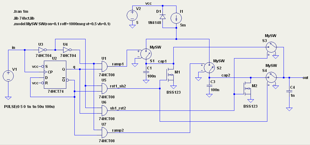
I used two inverters to partially account for delay in the flip-flop. This reduced glitching in the gate outputs.

Here are the waveforms (ignore the added voltages, they are just to separate the traces):-
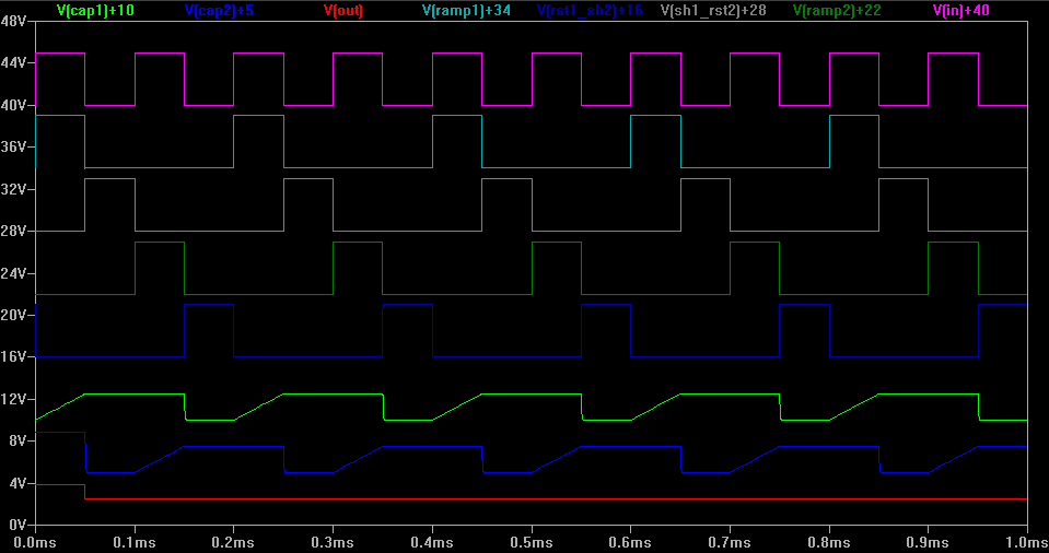
enter image description here

Note that I only made this circuit to explore the concept. I don't recommend using it in a practical application because there are better solutions.

How best to reduce the glitches?

Arrange digital timing delays so the gate outputs don't glitch. Make sure that there is sufficient time between processes (eg. don't reset ramp until well after its value has been transferred to the output). Put a capacitor on the output to hold the value while switching between integrator outputs.

Can R7 be dropped?

Better to put a resistor on both outputs. Then the circuit will be symmetrical and you can add some capacitance on the output to smooth out glitches without making the op amps unstable.

Final notes:

I have thought about using this technique before, but never had an application that made the added complexity worth it. Now that I see its limitations I am even less likely to use it. Why? Most PWM applications involve an MCU at some point. If it is producing the PWM then it may be easier to use a serial DAC, or not convert to analog at all (if another MCU will be receiving it). An MCU can also easily receive PWM and produce analog output via a DAC, using a lot less circuitry and higher practical accuracy.

In most cases a good analog filter can provide sufficiently smooth output with fast enough response time, and has the advantages of automatic calibration and adaptation to different PWM periods. This leaves little room for an advanced technique that suffers from other limitations that could be more serious (eg. failing dramatically at 0% and 100% PWM). Also there are ICs available that do the same job.
\$\endgroup\$
0
\$\begingroup\$

The logical approach is to a Vref near Vcc/2 , that is stable for single supply use. This is your virtual ground which you can use to level shift down to 0V with rail-to-rail Op Amps later.

Then integrate up on “1” and down on “0” with a track/hold buffer for each cycle. You want to avoid S/H glitches this way but still need a “brick” LP filter on the buffered output if this were to be used with BW limits.

  • always use a low dielectric constant cap for S/H caps to avoid the hysteresis effects. Metal film are preferred.

A more logical approach is to integrate digitally and e.g. 10 MHz counters = 3 decade resolution = 10 bit resolution of the PWM duty cycle glitch free using up/down counters. Or for 4 digit results use the ICM7242IPA or some other type with a DAC analog output of the counter

\$\endgroup\$
1
  • \$\begingroup\$ The Vcc/2 makes sense but I don't understand the proposed up-down integration. Do you just mean that the input will not be switched, so the integrator will be always running and the output will be the difference between the high and low segments? \$\endgroup\$
    – Reinderien
    Commented Jun 29, 2021 at 3:53

Your Answer

By clicking “Post Your Answer”, you agree to our terms of service and acknowledge you have read our privacy policy.

Not the answer you're looking for? Browse other questions tagged or ask your own question.