4
\$\begingroup\$

I have a 6-Layer board (See Design) which is an extension that is connected to a motherboard through a Board to Board Connector. The extension should provide: two USB 3.2 GEN 2 ports, two USB 2.0 ports, two HDMI ports, two mini-DP ports.

I want to decide on which layer to put the power planes (or polygons to be more accurate). I have 4 power voltages that should be available: 5VA, +3V3LAN, +3V3S, +3V3A.

on Bottom layer I have Intel I219 and I211 PHY and Ethernet Controller. on Top Layer I have B2B connector that delivers the 4 voltages (5VA, +3V3LAN, +3V3S, +3V3A) and all the signals (PCIE, MDI, etc.), and they all come from the motherboard.

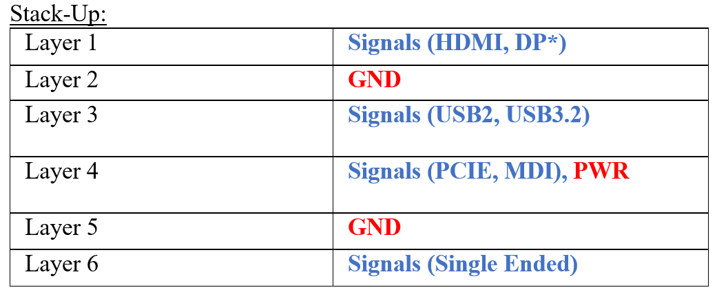
Here is the layers description and the way I chose the signal and GND planes:

enter image description here enter image description here

I want to know where is best place to put the Power planes. I understood that choosing Layer 2 and 5 as GND plane is a good way to create a Farady Cage, but how is this cage affected if the there are power polygons in the middle at layer 3 and 4? and how these polygons affect the Hi-Speed signals on layers 3,4?

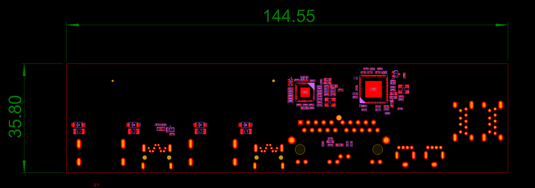
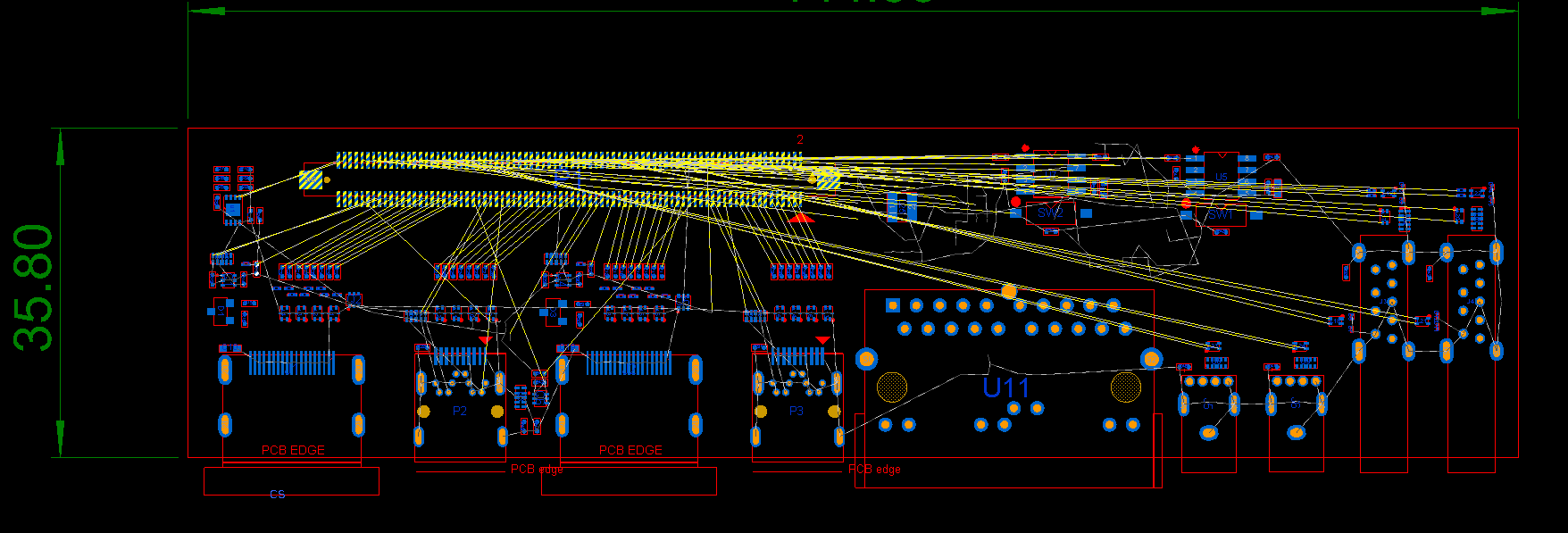
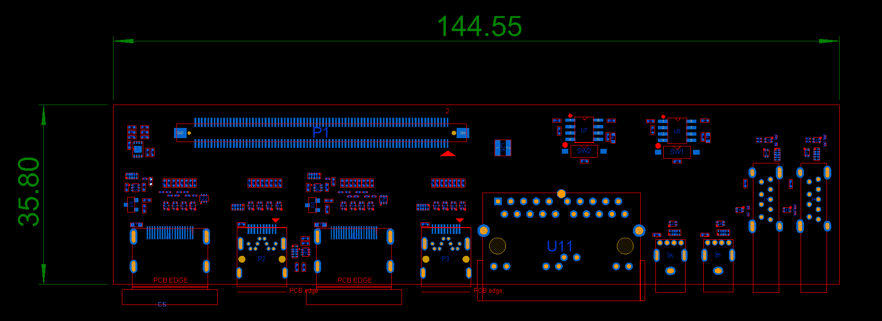
here is how the Layout placement looks like: Top Layer: enter image description here Bottom Layer: enter image description here Netlines (before routing) enter image description here
\$\endgroup\$
9
  • 1
    \$\begingroup\$ The HDMI ought to have an SMD CM choke to improve signal integrity from CM noise and impedance mismatch tolerances on board and cable. \$\endgroup\$
    – D.A.S.
    Commented Jul 24, 2021 at 15:21
  • \$\begingroup\$ It has, please see the design I added. \$\endgroup\$ Commented Jul 24, 2021 at 15:28
  • 1
    \$\begingroup\$ I didn't make an answer. I just made an observation/comment. \$\endgroup\$
    – Andy aka
    Commented Jul 24, 2021 at 15:32
  • 1
    \$\begingroup\$ Another thing to consider: Pairs of layers on a multi-layer board are manufactured on very thin two-layer boards, then sandwiched with insulating material in between. High-speed signals and ground should be put on opposite sides of such a two-layer board for impedance control. This means that PCIE/MDI should be on layer 6 with ground on layer 5. Non-critical stuff can go to the middle layers. \$\endgroup\$ Commented Jul 24, 2021 at 15:43
  • 1
    \$\begingroup\$ It can be done that way, or it might be (1) (2,3) (4,5) (6) where 1 and 6 are simply foil attached with prepreg. You'll need to specify the stackup, or at least talk to the board house. \$\endgroup\$
    – bitsmack
    Commented Jul 24, 2021 at 20:57

2 Answers 2

2
\$\begingroup\$

Your stackup looks good to me, though this conclusion only applies for this stackup. Other stackups with e.g. layers 3 and 4 tightly spaced will not work.

But with this stackup that you posted, the crosstalk between layers 3 and 4 should be absolutely minimal if at all detectable. Everything in layer 3 will be referred to layer 2 and everything in layer 4 to layer 5.

If you have a signal in 3 and a power poly in 4, consequently, it will have pretty minimal coupling and there is no problem routing over edges of the power poly, simple because the signal is fully referred to layer 2 and doesn’t "see" the power poly. Just compare the impedance of the signal if you a) have only gnd in 2 to b) when there is also copper in 4 additionally. there will be almost no difference. Think of an ant crawling on your ceiling: it doesnt care if there are holes in your floor because it is fully referred to the ceiling. The ant is layer 3, ceiling layer 2 and floor layer 4.

The second question is if signals in 4 care about the power poly in 4. Again, not a lot, if you keep the signals at least about 15 mil (3 H) away from the poly.

Therefore, I consider 3 and 4 the best layers for your power polys, because you can bring the poly right under the ICs and have minimum supply inductance.

Just make sure that when you cross anything from the top layer triplet to bottom, that you provide sufficient gnd vias nearby, so return currents can transition between layers 2 and 5. Crossing without GND vias is only ok, if you cross between 1 and 3 or between 4 and 6. However, tracewidths must be different on layers 1 and 3, but you are probably aware of that and impedance calculation when you design such a board..:-)

\$\endgroup\$
1
\$\begingroup\$

Here is the 6 Layer stack up I would prefer.

Layer 1 - Signal/Power
Layer 2 - Ground
Layer 3 - Signal/Power
Layer 4 - Ground/Signal
Layer 5 - Ground
Layer 6 - Signal/Power

Here is my layer stack up image with thickness of dielectric between the copper layers. My Total PCB thickness is around 1.2mm.

enter image description here

Let me justify why I prefer this type of stack up over others.

First of all, when you are routing your PCB, you have to route every signal with respect to the ground like you actually mean it. You cannot route them randomly and say "Hey it will find it's ground". No, that's not how a circuit works. For a circuit to work properly, every signal needs to have an intentional low impedance ground nearby.

Now if you see my stack up, you'll notice every signal and power plane on my PCB has reference ground plane close by.

I'll make sure I never route any signal on Layers 2 and 5. Other layers (L1, L3, L4 and L6) are left at my discretion. I can use them for routing signals and as a power polygons.

\$\endgroup\$
2
  • \$\begingroup\$ hmm. but your signals on layer 4 have no reference Ground plane?! otherwise I also like this stackup but it works only for doublets of closely spaced copper layers. The OP has two triplets instead. \$\endgroup\$
    – tobalt
    Commented Aug 19, 2021 at 4:31
  • \$\begingroup\$ When routing through Layer4, you need to make sure there is always a ground trace or ground pour nearby. I will post some pictures in my next post on how I accomplished it. \$\endgroup\$
    – Cactus1549
    Commented Aug 19, 2021 at 7:36

Your Answer

By clicking “Post Your Answer”, you agree to our terms of service and acknowledge you have read our privacy policy.

Not the answer you're looking for? Browse other questions tagged or ask your own question.