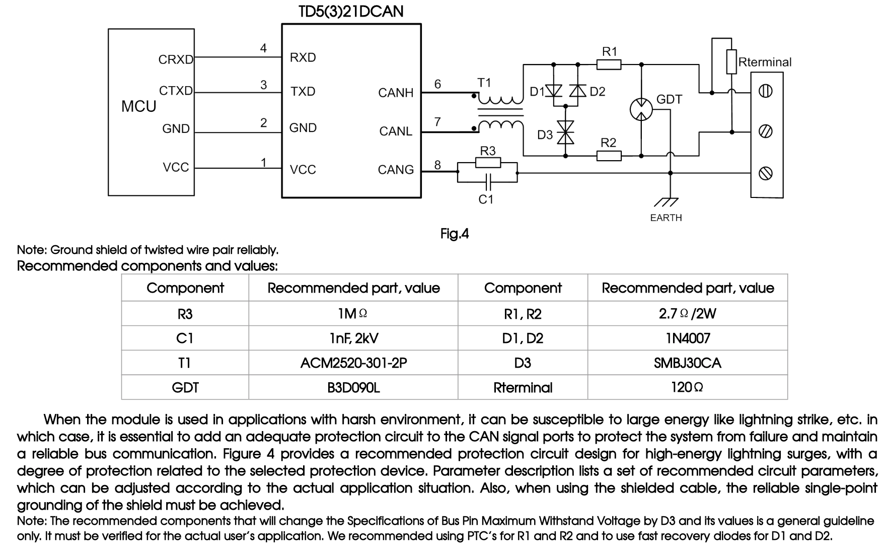
I think that the protection circuit has to be treated with suspicion. I say this because the circuit has a GDT as the first line of protection and, that doesn't mean that it's there to protect against puny levels of ESD but, "more muscular" indirect lightning surges (as per the words below the circuit).
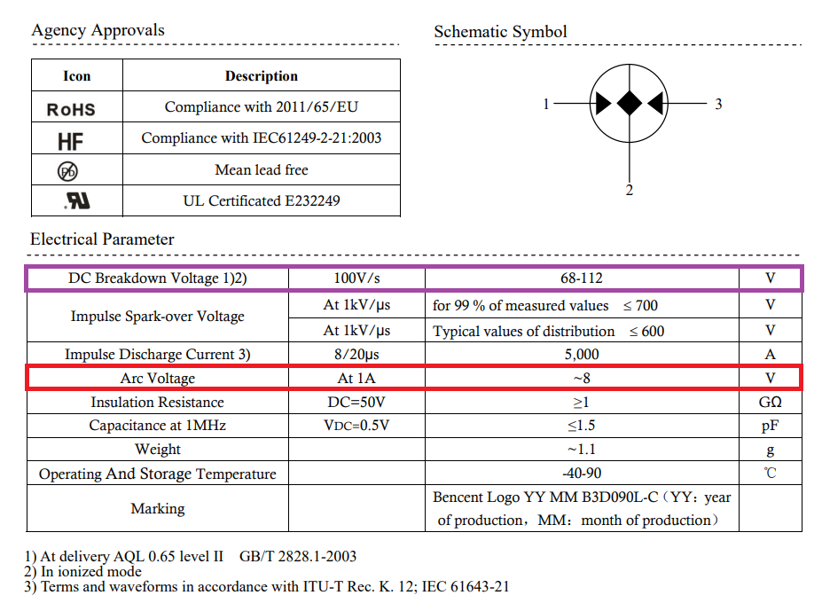
Now, indirect lightning surges are a totally different game when it comes to rating components and, the GDT used is a good example of a "muscle" device. Once triggered (it can take several microseconds to activate) it will clamp down to about 8 volts (see red below): -

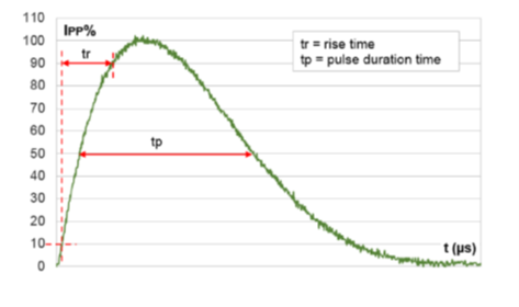
To trigger the device takes a DC value of about 68 volts to 112 volts (purple box above) and here's where the whole protection scheme is on shaky ground. For a few microseconds there might be a massive current surge into the TVS diode. This is because a GDT just does not respond that quickly. During this short time the terminal voltage might reach several hundreds of volts. The GDT data sheet suggests that the impulse spark-over voltage might be as high as 700 volts for an impulse rising at 1 kV per μs.
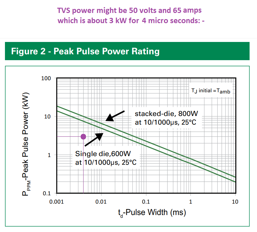
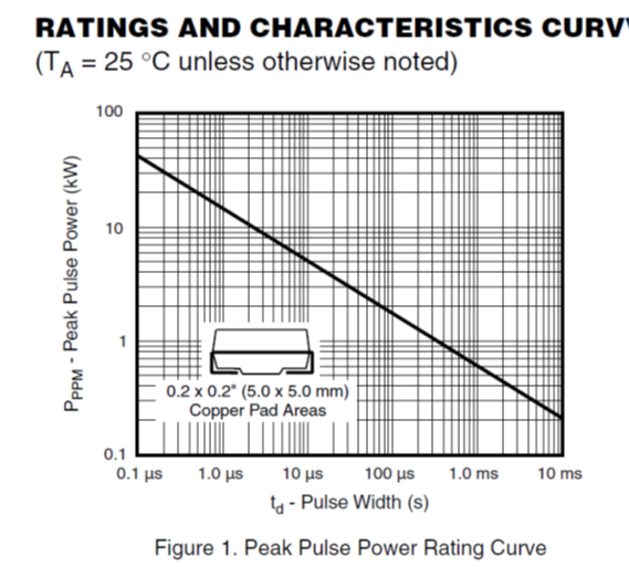
So somewhere between an impulse of 100 volts per second and 1 kV per microsecond you will see a terminal voltage that might be many hundreds of volts. I could make an estimation of 400 volts for 4 μs. During that time the peak current into the TVS will only be limited by the 2 watt 2.7 Ω resistors in each leg. Given that the TVS has a maximum clamping voltage of 48.4 volts (at a peak current of 12.4 amps) means about 350 volts across the two 2.7 Ω resistors.
That's a peak current of about 65 amps: -

So, the TVS can handle it but, the series 1N4007 diodes offer no evidence that they can handle that sort of current. So, when you ask this: -
What is the purpose of D1 and D2?
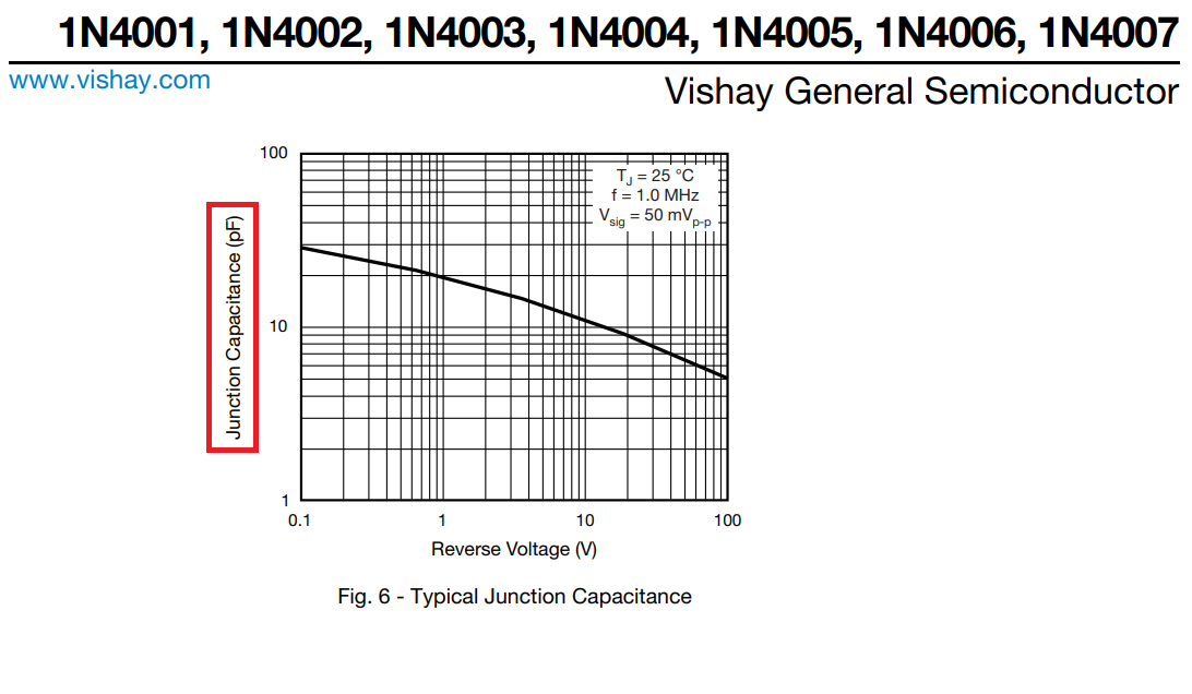
I have to say that it looks like some bodge to fix something and I doubt that they will survive any meaningful lightning protection test. As a guess, I would say that the self-capacitance of the TVS of several nano farads might disrupt data sufficiently and, the forward voltage drop of the 1N4007 gives just enough extra headroom on data amplitude to ensure that it works. The 1N4007 has a reverse capacitance of only a few pF so it could improve data integrity against the backdrop of excessive natural capacitance in the TVS diode: -

What is the purpose of R1 and R2?
I've explained that earlier i.e. they limit current into the TVS and protect it but, you need to ensure that those resistors can take a massive surge power of over 10 kW each for a few microseconds.
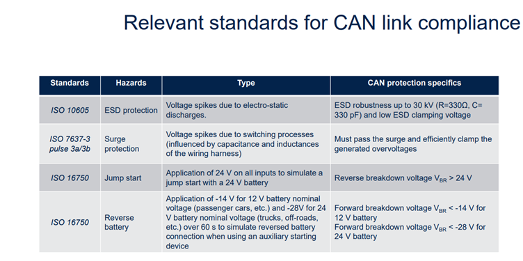
And finally, with any over-voltage protection scheme offered, there should be a statement about what it is intended to protect against i.e. the threat should be named explicitly (as per EN 61000-4-5 for instance). The words below the Mornsun circuit are these: -

And, they are insufficient in my opinion.

