6
\$\begingroup\$

I'm unable to find a definitive answer to this (trust me, I've looked, unless it's right under my snout) so please do point out the correct answer if I have. I'll feel foolish but at least then I'll know!

This isn't about mirrors, etc. but more specifically something I must have missed although I'm sure it must have something to do with output impedance, I can't wrap my head around the idea that we always (seem) to use NPN transistors (or N-type mosfets) to sink current from a load and vice versa. Even writing this, I'm starting to question if I have that the right way around... My poor noodle is all a tizzy over this.

Assuming the device is saturated (BJT) then all the current flows through the circuit equally with a little bit extra coming via the base-emitter junction to drive it. With a beta of 100 that's probably a fairly insignificant quantity.

My best guess was this would apply with split rail voltages (referenced to ground) but I've seen NPN and PNPs used as sources and sinks in single rail applications without explanation and that's where I'm stumped.

What am I missing here? It must be so obvious that I can't see it.

\$\endgroup\$
7
  • 1
    \$\begingroup\$ In normal conditions when the NPN transistor emitter is at GND and the load at the collector side. The collector current can only flow from "collector to emitter". The collector can only "sink" current. But if we put a load between the emitter and GND and collector to the power supply. Now notice that now the emitter can "source" the current and cannot "sink" current (current can only flow out of the emitter and never flow into the emitter. \$\endgroup\$
    – G36
    Commented Aug 25, 2021 at 20:44
  • 2
    \$\begingroup\$ I can use an NPN to make a current sourcing or a current sinking circuit. The same applies to a PNP. So your question's statement that PNPs source and NPNs sink is wrong. \$\endgroup\$ Commented Aug 25, 2021 at 20:44
  • \$\begingroup\$ And this statement is true "PNP transistors source current and NPN transistors sink it". In the case when NPN or PNP is connecter as a CE amplifier. Emitter at GND load at collector for NPN transistor. And for PNP when the emitter is at Vcc and the load is at the collector side. \$\endgroup\$
    – G36
    Commented Aug 25, 2021 at 20:48
  • \$\begingroup\$ @marco, draw a schematic with the tool (edit your question) or find a circuit that matches your description. \$\endgroup\$
    – Voltage Spike
    Commented Aug 25, 2021 at 21:19
  • 2
    \$\begingroup\$ they are used as they are because one lead needs to be a lower voltage than the other, which lends itself to sink/source but doesn't mandate it per-se. \$\endgroup\$
    – dandavis
    Commented Aug 25, 2021 at 21:35

3 Answers 3

10
\$\begingroup\$

This is because it's more typical to connect the load to the collector. You can use the emitter as an output, but that has certain limitations...the voltage gain will always be 1 in an analog emitter follower configuration, and in either an analog or switching configuration, driving the load from the emitter requires either a compromise in output range due to B-E drop, or the addition of some kind of boost circuitry to produce base voltages outside the supply rails. Sometimes the higher mobility of NPN (or N-channel) devices makes it worth implementing a boost mechanism, but most designs use complementary collector driving schemes.

\$\endgroup\$
1
  • \$\begingroup\$ Thank you Christobol, that makes a lot more sense. Perhaps I gave the other folks here the idea that I was more of a noob than I am, which is entirely my fault of course. I just got this idea into my head that I was missing something (i.e. what you've pointed out) and I couldn't see the wood for the major deciduous forest. \$\endgroup\$
    – Marc Draco
    Commented Aug 26, 2021 at 1:07
12
\$\begingroup\$

Have you ever heard of an emitter follower?

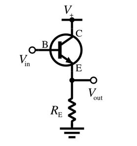
An NPN transistor connected in the emitter follower configuration sources current:

This figure is from the Wikipedia page on the common collector (emitter follower) circuit:

enter image description here

It sources current just fine.

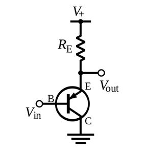
This emitter follower (also from the Wikipedia page) made with a PNP transistor sinks current:

enter image description here

Your assumption that an NPN always sinks current and a PNP always sources current is incorrect.

The transistors can do either. How they are connected makes the difference.

\$\endgroup\$
7
  • 2
    \$\begingroup\$ In fact, they always do both. All the current that goes in one place goes out another place. \$\endgroup\$ Commented Aug 25, 2021 at 20:51
  • \$\begingroup\$ I'll have to find somewhere that shows this in more detail and I know most "basic" circuits. I do know how to Google and I do own a (rather worn) copy of Art of Electronics (2nd Edition). I guess this must be more to do with convention than anything else since Kirchhoff's current law has to apply - I learned that one >30 years ago. \$\endgroup\$
    – Marc Draco
    Commented Aug 26, 2021 at 1:04
  • \$\begingroup\$ Such a shame this wasn't the accepted answer. \$\endgroup\$ Commented Aug 26, 2021 at 4:31
  • 2
    \$\begingroup\$ It would be worth pointing out the characteristics of the circuit are different! \$\endgroup\$ Commented Aug 26, 2021 at 9:05
  • 2
    \$\begingroup\$ This doesn't really address OP's confusion, though. In control circuits OP's point is generally true - that NPN and PNP are used for sinking and sourcing, respectively, and for good reasons - you can't generally build circuits the other way around that work. I think this answer fails to appreciate the fields where OP's oversimplified claim is generally true - anyone working in controls would generally live by the same rule of thumb. These emitter followers are special cases with hard limitations that make them unsuitable in many (most?) applications where you need to sink or source current. \$\endgroup\$
    – J...
    Commented Aug 26, 2021 at 12:07
0
\$\begingroup\$

I think the only correct way is to go back to the electrical equivalent of a BJT (or mosfet) in different configurations. Reading those (a bit hard... I agree..) formulas You can see that You can have different practical behaviours.

So engineers will choose formulas based on the scope: You will use a different equivalent circuit with wanted parameters, (gain / output voltage / current output / output impedance and so on..). Chosen the required parameters, you will have to adopt the corresponding circuit (common emitter/collector or even base)

to sum up: you use a circuit not reasoning how current flows ( up/down/whatever...) but once decided the application of your circuit that fits better.

\$\endgroup\$

Your Answer

By clicking “Post Your Answer”, you agree to our terms of service and acknowledge you have read our privacy policy.

Not the answer you're looking for? Browse other questions tagged or ask your own question.