1
\$\begingroup\$

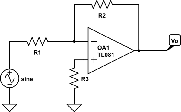
I'm trying to figure the effect of adding a resistance at the non-inverting input of a inverting amplifier.
schematic

simulate this circuit – Schematic created using CircuitLab

How can introduce it in the derivation of the transfer function?

I understand that when there is a voltage source at the non-inverting input and the resistor it makes the voltage level at both inputs are the same (like some kind of clip.)

In this case if there is voltage source in the + input.

\$I_{+}=\frac{0-V_{source}}{R_{3}}=0A\$
since there is no current entering the op-amp, but in the case of the diagram, how can represent the + input in math form so it can be added to the derivation of the standard non-inverting amplifier?

\$\endgroup\$
3
  • 3
    \$\begingroup\$ Search: opamp input bias compensation. R3=R1 || R2 \$\endgroup\$ Commented Sep 5, 2021 at 16:02
  • 2
    \$\begingroup\$ R3 also adds noise. \$\endgroup\$
    – tobalt
    Commented Sep 5, 2021 at 16:41
  • 1
    \$\begingroup\$ R3 has no meaning for me. As far as I know, no circuit with an additional R3 is mentioned in the literature. Except for the differential amplifier. Then of course you need a resistor so as not to short your signal. \$\endgroup\$
    – arnisz
    Commented Sep 5, 2021 at 16:55

3 Answers 3

6
\$\begingroup\$

since there is no current entering the op-amp

There can be input bias currents.

Both input bias currents are usually fairly equal in a lot of op-amps and so, to counter the error they produce at specifically the inverting input, a resistor equal to R1||R2 is placed in series with the non-inverting input. Now, the two errors largely cancel.

However, many op-amps don't require this because their input bias currents are sub-pico-amp (JFET or MOSFET type inputs). Those that can benefit are generally those op-amps that use BJTs in their input stage.

\$\endgroup\$
4
  • 3
    \$\begingroup\$ I agree that the circuit with the added resistor is used for opamps that use BJT transistors at the inputs, the resistor is not needed for the Jfet inputs on the TL081 opamp. \$\endgroup\$
    – Audioguru
    Commented Sep 5, 2021 at 15:51
  • 1
    \$\begingroup\$ Hey Andy I am curious. What if one didn't choose a resistor equal to R1||R2, but instead chose something in the extremes like \$R=1\text{m}\Omega \$ or \$R=10\text{M}\Omega \$. Would it have unwanted effects on the circuit? \$\endgroup\$
    – Carl
    Commented Sep 5, 2021 at 16:47
  • 2
    \$\begingroup\$ @Carl in the low extreme, the input bias current would produce a small offset voltage error of one polarity. In the high extreme, it's likely that a much bigger error offset voltage would be produced in the opposite direction. \$\endgroup\$
    – Andy aka
    Commented Sep 5, 2021 at 16:50
  • 2
    \$\begingroup\$ @Andyaka I think I intuitively understand the first extreme's effect. I don't quite understand the other, perhaps I should do a quick simulation. Anyway, thanks for answering my question, you have my upvote. \$\endgroup\$
    – Carl
    Commented Sep 5, 2021 at 16:53
1
\$\begingroup\$

I did not do a thorough check on a laboratory mockup.

I would like to give an answer to the question, taking into account an additional element which is often negligible and neglected.

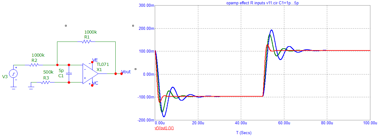
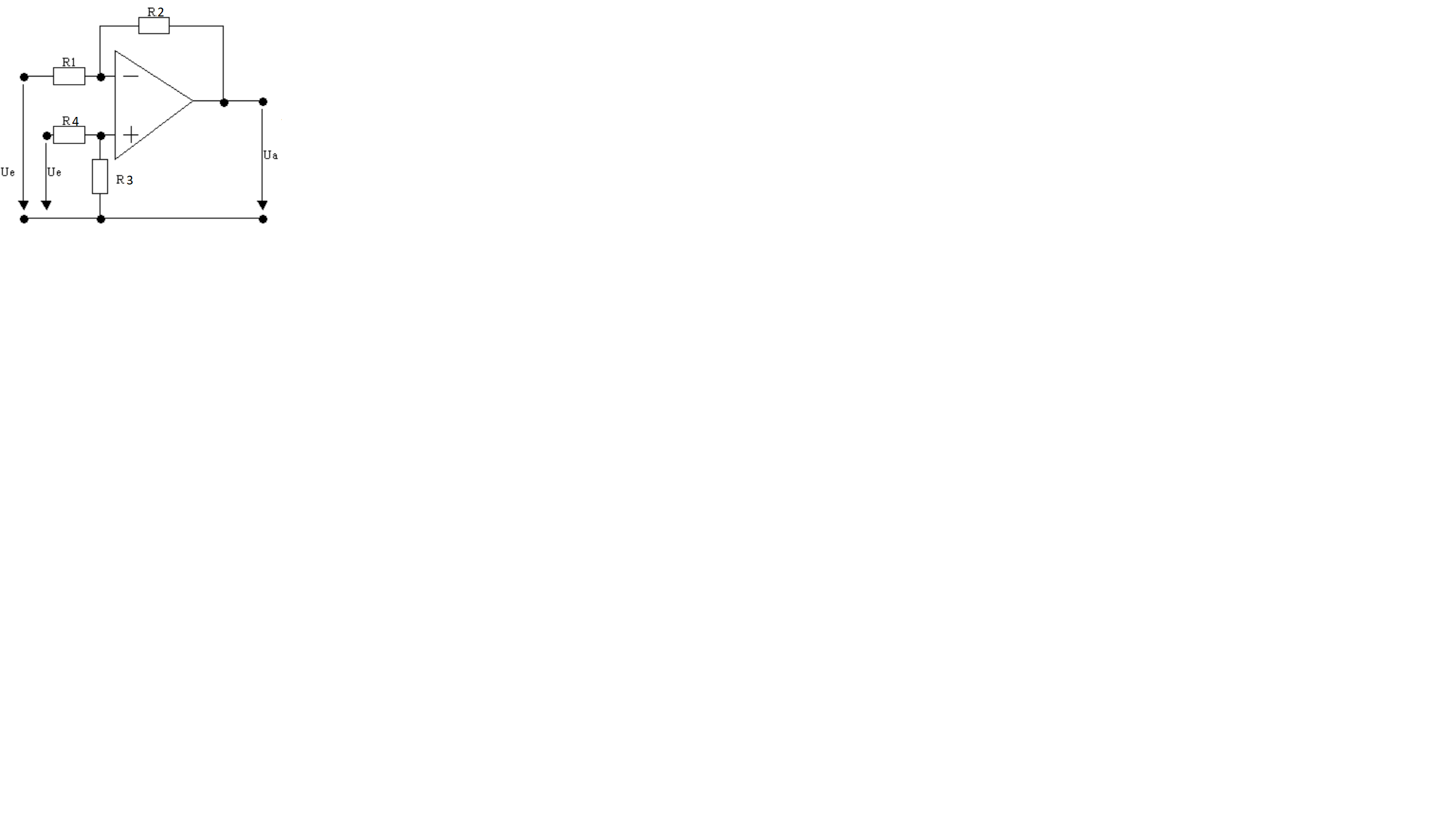
Suppose that one uses resistive elements of rather high value but not that much. R1 and R2 are equal to 1 MOhm, R3 equal to 500 kOhm ( or 0). Neglected disturbing element: capacitance between the + and - inputs of the operational amplifier (this situation can occur on a test board with multiple "capacitive" connections, or other circumstances). Simulation results below with a capacitor of only 1pF to 5pF. You can see the ringing that occurs. Negligible ?

enter image description here

enter image description here

\$\endgroup\$
-1
\$\begingroup\$

According the simulation the inverting input of your op-amp is virtually ground so R1 represents the input resistance of your amplifier. The current through R1 is the same as R2 but opposite direction. Changing the Value of R3 has no effect.

Given input voltage = 1.5 V, R1 = 1 kΩ, R2 = 2 kΩ and R3 = 3kΩ

IR1 = 1.5/1k --> 1.5 mA = I(R2)

Uout = -1.5 mA × 2k = -3 V

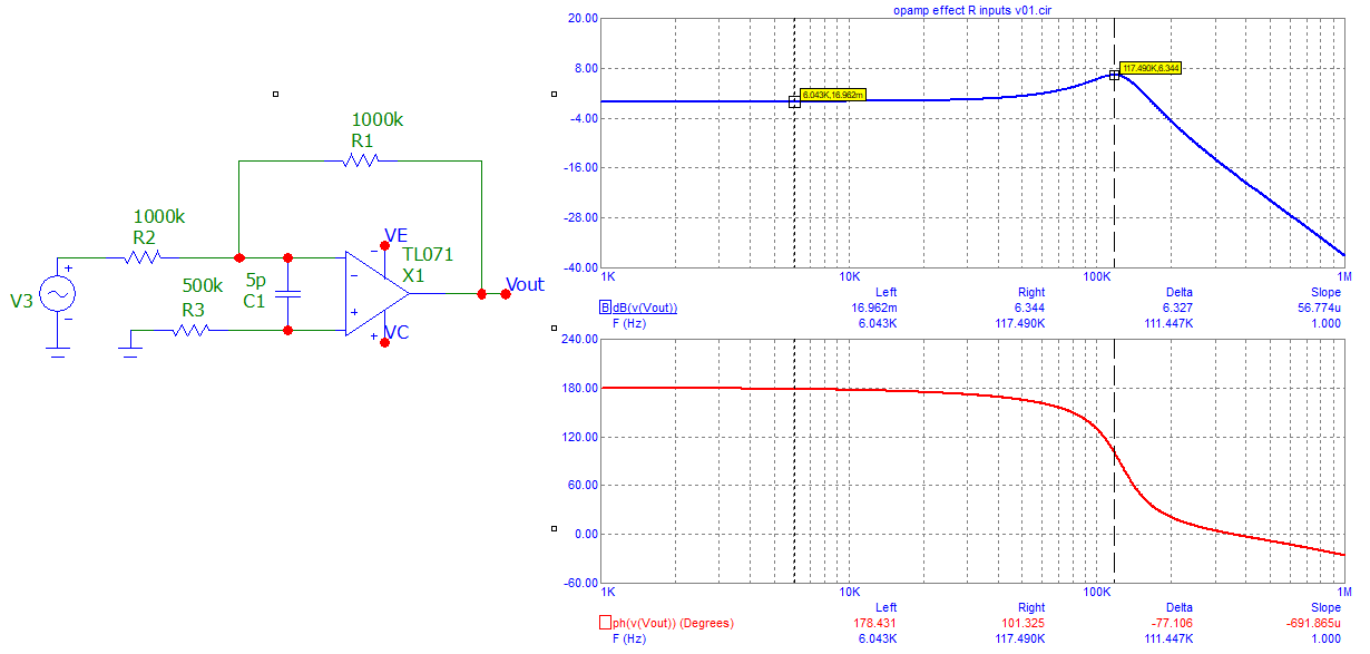
R3 is required if you want to build a differential Amp like

DiffAmp
(source: szathmary.net)

\$\endgroup\$
2
  • 1
    \$\begingroup\$ R3 is required to cancel the effect of bias currents on the '-' input. If you leave out R3 then the '-' bias current will cause an offset because it will pass through R1 and R2. See Andy's answer for an explanation. \$\endgroup\$
    – Transistor
    Commented Sep 5, 2021 at 17:10
  • 1
    \$\begingroup\$ Tip: You can add in schematic diagram using the CircuitLab button on the editor toolbar. Double-click a component to edit its properties. 'R' = rotate, 'H' = horizontal flip. 'V' = vertical flip. Note that when you use the CircuitLab button on the editor toolbar and "Save and Insert" on the editor an editable schematic is saved in your post. That makes it easy for us to copy and edit in our answers. You don't need a CircuitLab account, no screengrabs, no image uploads, no background grid. \$\endgroup\$
    – Transistor
    Commented Sep 5, 2021 at 17:11

Your Answer

By clicking “Post Your Answer”, you agree to our terms of service and acknowledge you have read our privacy policy.

Not the answer you're looking for? Browse other questions tagged or ask your own question.