Relays are switches controlled by a current. Transistors are switches... controlled by a current. FETs are switches... controlled by a voltage.
Gates are constructed by combining switches in various ways, in parallel or serial, to form pull-up and pull-down networks.
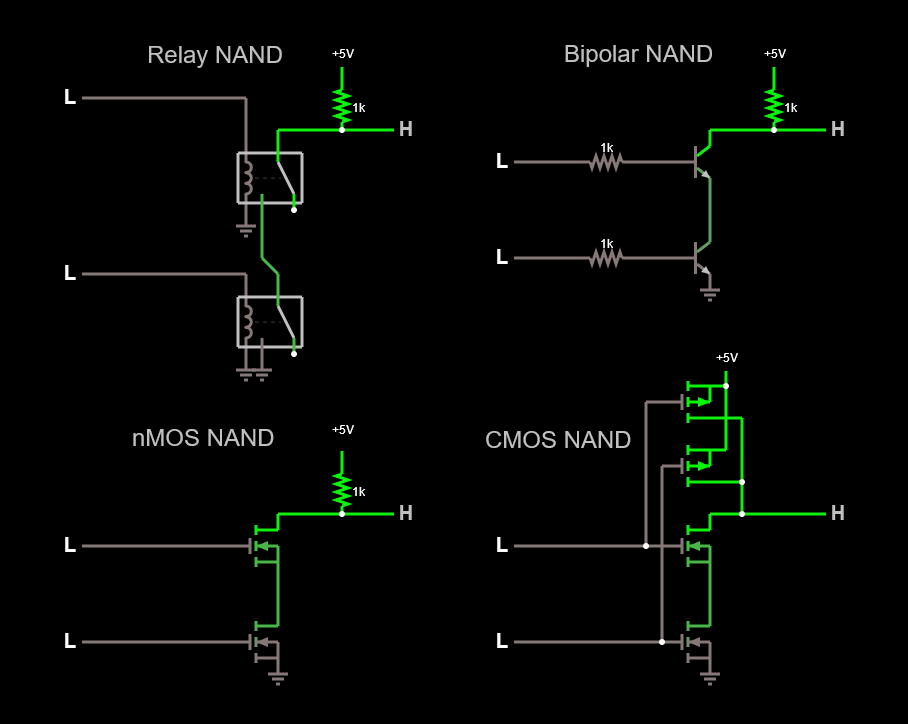
Example - NAND Gate (2 switches in series, simulate it here):

All four of these work the same way, using a pair of switches wired in series that pulls down the output to GND when both inputs are HIGH:
Relay - both coils on close two switches in series to pull the output down. Resistor pulls up otherwise.
Transistor - both NPNs are on, pulling the output down. Resistor pulls up otherwise.
nMOS - both nFETs are on, pulling the network down. Resistor pulls up otherwise.
CMOS - both nFETs are on, pulling the network down. One or both pFETs pull up otherwise.
Ultimately, all the semiconductor gates shown here drive the outside world with the collector (bipolar) or drain (MOS), sourcing power from the supply or ground. They work that way because that’s the easiest way to bias them and get a strong, close-to-the-rail drive without loading the inputs. In other words, they also buffer the inputs.
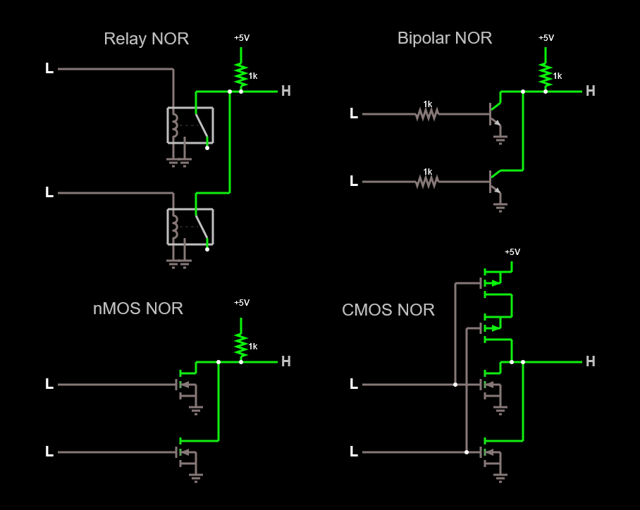
Continuing, NOR gates work the same way, but with switches wired in parallel on the pull-down side (simulate it here):

In both cases, CMOS is set apart from the others in that it uses an active pull-up, that exploits the opposite control polarity of the pFET gate to form a complementary switch to the nFETs on the low side.
You'll also notice in the sim that the CMOS gates use almost no current, because the pull-up and pull-down are controlled so that they don't turn on at the same time. That's the key to CMOS low power dissipation: no standby current, regardless of the logic level.
So while seemingly more complicated, requiring 4 elements instead of 2, CMOS zero-standby current and rail-to-rail drive offer huge advantages for large chips, which is why it's the dominant logic type in use today.
Now, you asked about using a ‘collector’ in series with another ‘collector’ to pass a signal. The NAND structures do that, but there’s a type of logic that takes it a step further: the transmission gate. These are most easily realized in CMOS, and are used to form elements like multiplexers, demultiplexers, and latches.
Transmission gates can also be used for logic, much like the relays you used over at nandland. And like relays, they have a neat party trick: they can pass digital or analog signals in both directions transparently, like a physical switch.
Finally, let's touch on contemporary bipolar logic. What is shown above for 'bipolar' is called 'RTL', or resistor-transistor logic. It was an early logic family developed in the 1960s, which saw application in the Apollo Guidance Computer as a 3-input NOR gate.
Contemporary bipolar logic, called TTL, or transistor-transistor logic, is a bit more complex. TTL uses transistors in series and in parallel in some creative ways to achieve lower power and better performance than its predecessors. Beginning with its introduction in the late 1960s up until the mid-1980s, most systems were built with it.
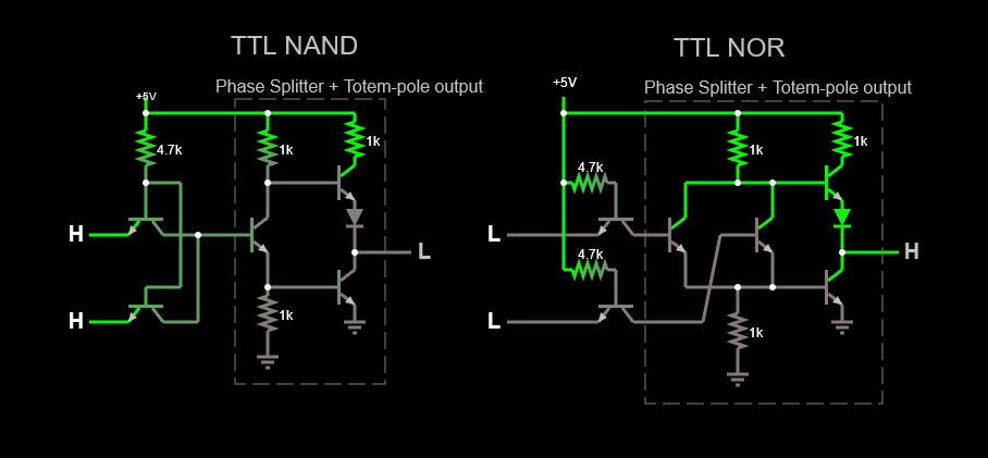
Below is what the guts of TTL NAND and NOR actually look like (simulate it here)

TTL inputs use a 'common base' NPN with inputs applied on the emitters. This is passed through to the collectors and on to the next stage buffer bases. After that, there's some voodoo going on: a phase splitter that allows the circuits to use only NPN transistors in the output stage.
With TTL there's some static current draw in certain states, and of course the inputs source current (100s of uA) when pulled low. You can observe that in the simulation.
Another bipolar logic family, called ECL or emitter-coupled logic, offered a higher-performance option for speed-critical designs. It was notoriously power-hungry, used weird power supplies and differential signals. Its most famous use was for the CRAY-1 and CRAY-2 supercomputers. Try a quick sim here: http://www.falstad.com/circuit/e-eclnor.html

