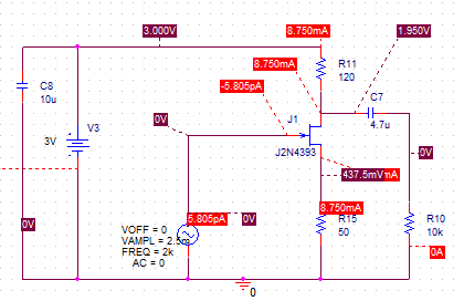
While simulating a basic common source JFET amp I found that eliminating the input capacitor improved the gain of the circuit dramatically. This is because without the input capacitor, the gate voltage is held to ground by the VOFF = 0 of the VSIN source. See figure 1.
Figure above shows the good biasing with no input capacitor and Vg = 0
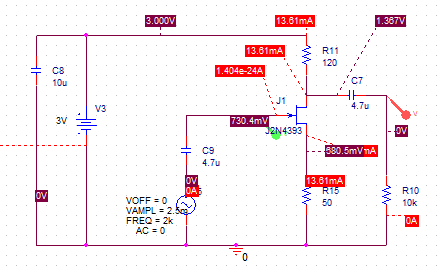
When the capacitor is included, this DC Offset VOFF is blocked by the input capacitor. So the gate voltage is allowed to float. Figure 2 shows that with the capacitor in place, the gate voltage Vg ~ 730mV. This changes the Q point of the JFET, putting it into the linear region and killing all good amplifier behavior.
Figure above shows Vg = 730mV with signal and cap
Figure above shows Vg = 730mV with no signal and cap
This made me curious as to where this ~730mV are coming from. Eliminating the VSIN source entirely did not change Vg = 730mV. So the presence of this gate voltage is caused by the supply voltage. Since the JFET is a depletion-mode device, it will conduct with no gate voltage applied. So when the supply voltage is applied across the drain and source of the JFET, the JFET will conduct. Since the drain of the FET will be much higher than the Gate voltage, Vdg > 0, This is like a reverse bias between the drain (connected to N-type channel) and gate (connected to P type well). Reverse biasing this p-n junction increases the voltage barrier across the junction. So the gate voltage present Vg is caused by the voltage drop Vdg due to the reverse biased PN junction. This does not sit well with me and I would like to better understand what is happening.
I tried a transient simulation using a VPULSE supply to see how the circuit behaves if the supply voltage is gradually increased instead of being an instantaneously present VDC supply. This experiment (figure 3 + 4) showed that the gate voltage only went to 1.8uV. Much less than the expected 730mV. What is going on here? Why is the DC bias so different when the supply voltage is pulsed from 0 to 3 instead of being a constant DC source?
Figure above shows pulsed supply with input cap does not produce the Vg = 730mV
Figure above shows gate voltage plot where Vg goes to 1.8uV. Not close to expected 730mV.
What is causing this behavior? What causes the gate to be biased at 730mV? Can anyone explain the DC bias being different for the VPULSE vs VDC supply? Thank you


