2
\$\begingroup\$

I am developing an H-bridge for use with 48VDC brushed motors. The bridge is implemented with discrete DPAK N-channel MOSFET transistors driven by an HIP4081AIBZ. I have not yet fitted RC snubbers across the FETs (although my board has pads for them, I just need to characterize the board to calculate part sizes), nor have I added any bypass capacitors across the motor (C8-C10 in the attached schematic).

Presently I am only driving one half of the bridge with PWM, Q2 & Q3. That means that during the PWM "on" period, the motor receives power and during the "off" period it coasts. I have provisions in the controller for this bridge to drive it in complimentary mode. That is, Q2 & Q3 on together in the "on" portion of the PWM signal, then Q1 & Q4 on together in the "off" portion of the PWM signal. Again, for now I am just PWMing Q2 & Q3 and leaving Q1 & Q4 off.

However, I am experiencing an interesting problem. As motor speed increases, Vgs on the high-side FETs drops, presumably due to motor regeneration during deceleration in the "off" portion of the PWM signal. Eventually Vgs drops enough that Q3 won't even turn on any more and the bridge starts "hiccuping". Obviously this is not good.

I think the problem will go away once I drive the bridge in complimentary mode, as the FETS that are on in minority portion of the PWM cycle will provide a path for motor regeneration, clearing the way for the next majority portion of the cycle.

However, before I start blowing FETs I would like to get some input from others.

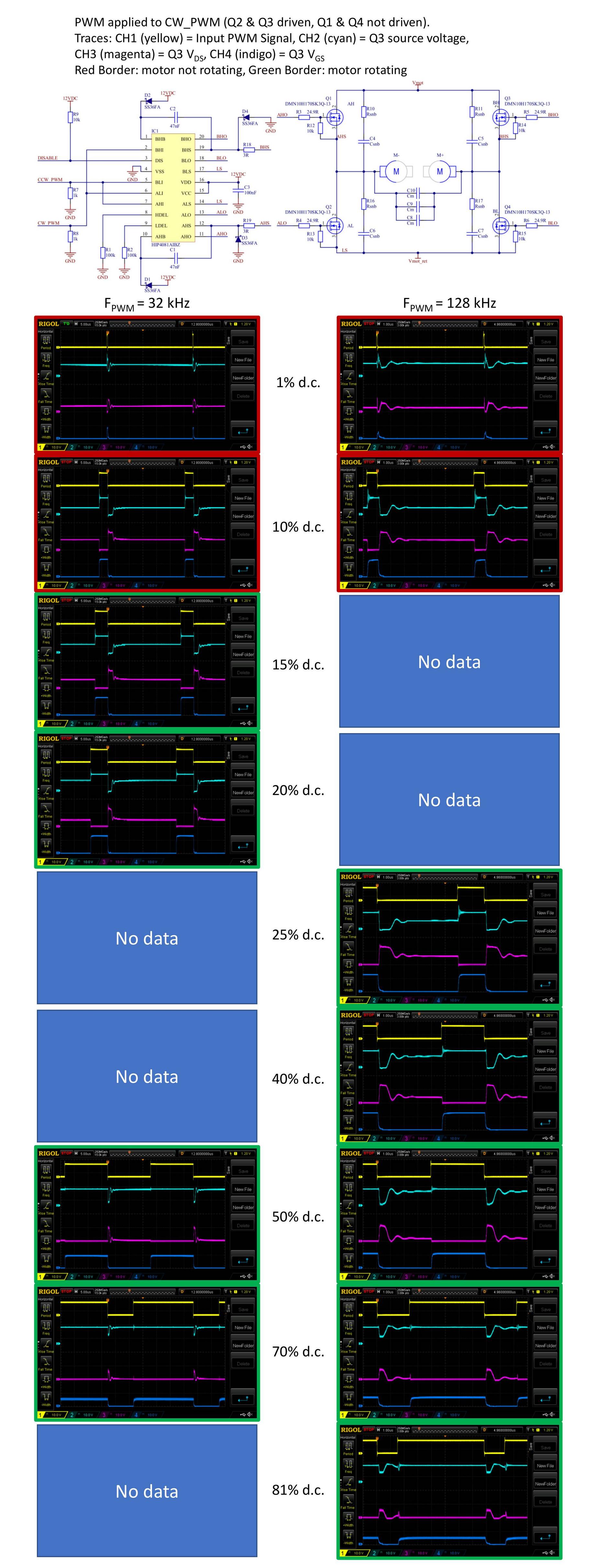
The attached image shows the circuit I am using, as well as several scope traces for various PWM duty cycles at two different PWM frequencies (32kHz & 128kHz). The Vgs problem appears at a lower duty cycle in the 32kHz setup, presumably because the motor is able to accelerate more in the longer on-times with the lower PWM frequency. The test setup and all of the traces are explained in the attached image (note that DISABLE is grounded during trials to enable the H-bridge driver).

Edit: Vmot_ret & ground are tied, even though this is not shown in the schematic. Schematic circuit, test parameters, & scope traces
\$\endgroup\$
8
  • \$\begingroup\$ "Q2 & Q3 on together in the "on" portion of the PWM signal, then Q1 & Q4 on together in the "off" portion of the PWM signal." - That would continuously reverse the motor direction at PWM frequency. Why do it? \$\endgroup\$ Oct 29, 2021 at 0:09
  • \$\begingroup\$ I don't quite understand your measuring setup. You measure: CH1: input PWM Signal - supposing it is referenced to GND. CH2- Q3 Source voltage, refeferenced to what? Is this Q4 Vds?. Now, the two grounds have to bonded together GND and motor return GND, in order for this circuit to work. IMO 128kHz is an overkill, not sure if anybody made such H-bridge with an ordinary component gate driver/MOSFET, it would be more suitable for SiC or GaN. Those 10k resistors from gate to source may significantly degrade the performance, why did you put them? \$\endgroup\$ Oct 29, 2021 at 6:47
  • \$\begingroup\$ What are those schottky diodes doing on the gate circuits? They just work as an additional capacitance. Why do you have double gate resistors, 3 + 24.9 Ohm? ake a choice and use only one resistor. Remove those diodes, remove 10k resistors, short 24.9 gate resistors, try. Update your question with details of measuring setup. Do you use differential probes? \$\endgroup\$ Oct 29, 2021 at 7:03
  • \$\begingroup\$ Re grounds: Vmot_ret and GND are connected, but it is not shown in this schematic; I neglected to show that when I stripped out the unnecessary features (connectors, etc.) from the schematic for this question. There is another board that stacks on top of this one that makes the connection, but inserts a small sense resistor between to allow for motor current measurement. I have added a note to this schematic to this effect. \$\endgroup\$
    – Chris
    Oct 29, 2021 at 17:11
  • \$\begingroup\$ Re Q2/Q3 on together in "on" portion of PWM, Q1/Q4 on together in "off" portion: This is so that at fast PWM frequencies 50% duty cycle leaves shaft stationary, and varying away from 50% on either side increases motor speed to full in either direction. This is the implementation recommended in the HIP4081 datasheet. It will result in circulating current at zero shaft speed, but this can be reduced by increasing PWM frequency, and disabling driver when not in use. Is this a bad idea? \$\endgroup\$
    – Chris
    Oct 29, 2021 at 17:15

3 Answers 3

1
\$\begingroup\$

Presently I am only driving one half of the bridge with PWM, Q2 & Q3. That means that during the PWM "on" period, the motor receives power and during the "off" period it coasts.

During the 'off' period, back-emf produced by the motor windings creates a negative voltage that increases until it reaches the supply voltage and turns on the body diodes of Q1 and Q4. When the motor is spinning the effective voltage that the back-emf needs to overcome is even higher because the motor is generating a positive voltage which subtracts from it.

The flywheel current rapidly removes energy from the windings, until the back-emf voltage drops below the supply voltage. At this point the body diodes turn off and the motor is effectively 'floating'. From then on the undamped inductance and parasitic capacitance create a decaying oscillation as the rest of the magnetic energy is dissipated.

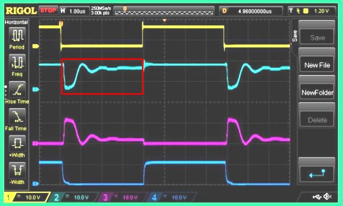
This is clearly visible in your "50% PWM 128 kHz" scope image. Here we see that the back-emf conduction period in this 'fast decay' mode is less than 1 μs.:-

enter image description here

Driver bootstrap capacitor C2 charges through D2 from +12 V, but only when the FET Source (node BHS) is close to ground. If it rises above ground then the charged voltage will reduce (to zero at ~11.4 V). Due to the fast back-emf decay the bootstrap capacitor doesn't have much time to charge, and it gets less at higher PWM ratio as the motor speed increases and produces more generator voltage which reduces the back-emf conduction time.

This problem can be solved by keeping Q2 turned on and applying 'half-bridge' drive to Q3 and Q4. This avoids the 'floating' problem, and is more efficient because the body diodes are bypassed most of the time.

\$\endgroup\$
6
  • \$\begingroup\$ Thank you for your response. This makes sense now that you have explained it. I'm a little uncertain about your proposed remedy, as driving both Q3 & Q4 would lead to shoot through, shorting the motor supply, no? The HIP4081 won't allow both Q3 & Q4 to be driven at the same time, either, but perhaps I'm misunderstanding. If I were to drive both sides (high signal on both CCW_PWM & CW_PWM), what the HIP4081 would do is turn on Q2 & Q4, but perhaps this is actually what you intend, as this would short the motor terminals and bring both to ground, allowing the caps to charge? \$\endgroup\$
    – Chris
    Oct 29, 2021 at 15:46
  • \$\begingroup\$ The HIP4081 has independent control of each FET, and has delays to prevent shoot-through, so it should be able to do it. Q3 and Q4 would be turned on alternately of course,not at the same time. \$\endgroup\$ Oct 29, 2021 at 19:15
  • \$\begingroup\$ Not so sure that your explanation is correct. What you red circled is that MOSFET keeps conducting when it shouldn't, there is no negative voltage caused by inductive dump. \$\endgroup\$ Oct 30, 2021 at 17:57
  • \$\begingroup\$ @MarkoBuršič I simulated it in LTspice. The waveforms matched. The 'MOSFET keeps conducting' is actually Q1 and Q4 body diodes conducting. With a +12V supply body diode current peaked at ~4A when the FETs turned off, and internal motor coil inductor voltage peaked at -23V (with lumped coil resistance of 1 ohm and 5.5V representing generator voltage at 50% rpm). \$\endgroup\$ Oct 30, 2021 at 18:46
  • \$\begingroup\$ @bruceabbott Thank you for the insight. If you don't mind me asking, how did you arrive at 5.5V for the motor generator voltage in your simulations, or did you just try many different voltages and the one that matched my traces the best? \$\endgroup\$
    – Chris
    Nov 1, 2021 at 17:31
1
\$\begingroup\$

A couple of issues:
first of all, you cannot only turn on and off Q1 & Q4 and leaving Q2&Q3 completely off. In this topology you should alternatively turn Q1&Q4 on(off) and Q2&Q3 off(on). Because the capacitors C1 & C2 (47nF) should be charged during the process. These caps are responsible to provide power for driving high-side Mosfets and they should be charged in every cycle through the on state of low-side Mosfets and are discharged during driving the high-side Mosfets, also you should make sure that the value of these caps are enough for driving the Mosfets.
Another issue: in this circuit, you have to have a common ground for both your driver and the full-bridge in the point of sources of Q2 & Q4.
Another point is that there's need for a timing gap (a delay) between turning OFF Q1 & Q4 and turning ON Q2 & Q3 and vice versa. It's harmful if you immediately turn off and turn on in the way you described in your text.

\$\endgroup\$
2
  • \$\begingroup\$ The HIP4081 inserts deadtime (set by R1 & R2); shoot through is not happening. There is common ground between the driver and the bridge (Vmot_ret is connected to gnd). The bootstrap caps recharge during the Q2 & Q3 off period - if anything they caps are oversized (measured droop < 1V), recharge in ~0.2uS. When Q2 & Q3 are off, the body diodes of Q1 & Q4 conduct for free wheeling (half bridge drive). What I'm seeing is due to motor generation during decel because if I lock the shaft it disappears. It's my intention to use complimentary PWM, so I will try that and report back. \$\endgroup\$
    – Chris
    Oct 28, 2021 at 23:26
  • \$\begingroup\$ I see your point now about how alternating Q2/Q3 and Q1/Q4 will help with bootstrap charging, in that it will alternately force the sources of Q2 & Q4 to ground, allowing the caps to charge. It's not that complimentary drive is necessary, per se, but it a side effect of it is that it high-side FETs sources are forced to ground (plus Vds of the low side FETs) whenever they are off. Thank you for your help. \$\endgroup\$
    – Chris
    Oct 29, 2021 at 19:09
0
\$\begingroup\$

schematic

simulate this circuit – Schematic created using CircuitLab

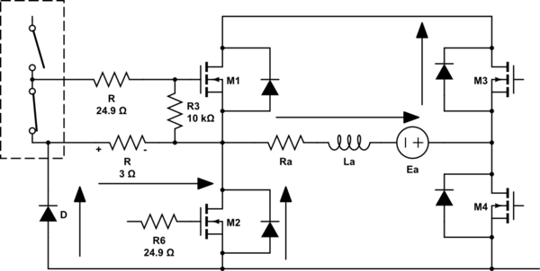
There are many issues in your design. First is not clear aboutt the function of diode and resistor on AHS, BHS gates. As you can see, a recirculating current could even turn on the MOSFET when it should be off.

When the M1 closes, the whole recirculating current, at first moment would pass through those R/D because the schottky diode has lower forward voltage than intrinsic diode of the MOSFET. This will generate a voltage drop on R that will turn the MOSFET on again.

The diode and resistor also adds unwanted resistance and capacitance in the gate circuit. I do think you are wrong, but you can prove otherwise with a scientific article or application note where this is described. Also it is not clear why do you use gate pull-down resistors, the driver needs more current to turn MOSFET on, so not very clever idea.

I do think you have understood, that lower transistor of the respective leg (half bridge) can't be in non-conductive mode all the time, because the bootstrapping won't work.

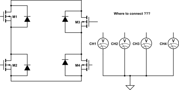
I have tried to understand the scope traces, but I am suspicious that they are not valid. You could use a schematics editor and draw how did you connect the scope.

schematic

simulate this circuit

How did you connect CH1 to CH4 to get Q3 Vgs, Vds, Vs and PWM input ??

\$\endgroup\$
1
  • \$\begingroup\$ to answer your question about how I was able to measure the various parameters simultaneously, I have used 100MHz differential scope probes on all signals except input PWM. I know that the negative terminals of normal probes are all tied. \$\endgroup\$
    – Chris
    Oct 31, 2021 at 17:04

Your Answer

By clicking “Post Your Answer”, you agree to our terms of service and acknowledge you have read our privacy policy.

Not the answer you're looking for? Browse other questions tagged or ask your own question.