2
\$\begingroup\$

I'm finalizing the routing for an eighteen-layer board that requires many, many differential-pair traces to run at speeds up to 16 Gbit/sec. (FYI: 100 Ω impedance, Isola I-Speed cores and prepreg.) These traces come from an MPSoC (BGA) with TX/RX pairs at 100 Ω impedance. All vias must be through-hole.

My design constraints limit me to roughly 3 mil trace gap while routing under the MPSoC due to the through-hole vias, then spread out to roughly 6 mil when the trace gap is no longer limited under the MPSoC.

I'm having trouble deciding whether my differential-trace pairs should spread out suddenly or gradually. I've read that in high-speed designs, trace width (not trace gap) will gradually fan out right before a pad to the pad width in order to minimize the sudden impedance change, similar to a tear-drop effect. Though taking this notion and extending it to trace gap seems logical, it poses two questions:

  1. Is this reasoning even correct? A specifically unnamed eval board with trace pairs running at much higher bandwidth than mine (see below) employs a "sudden" gap-change, regardless of whether the trace pairs are A) "regular" high-speed using 45° bends, or B) "super duper" high speed and requiring curved traces.

  2. What is too large of a differential-trace pair length to be changing the gap? If my reasoning is correct, there is no maximum "change in gap" length, but this doesn't feel right intuitively.

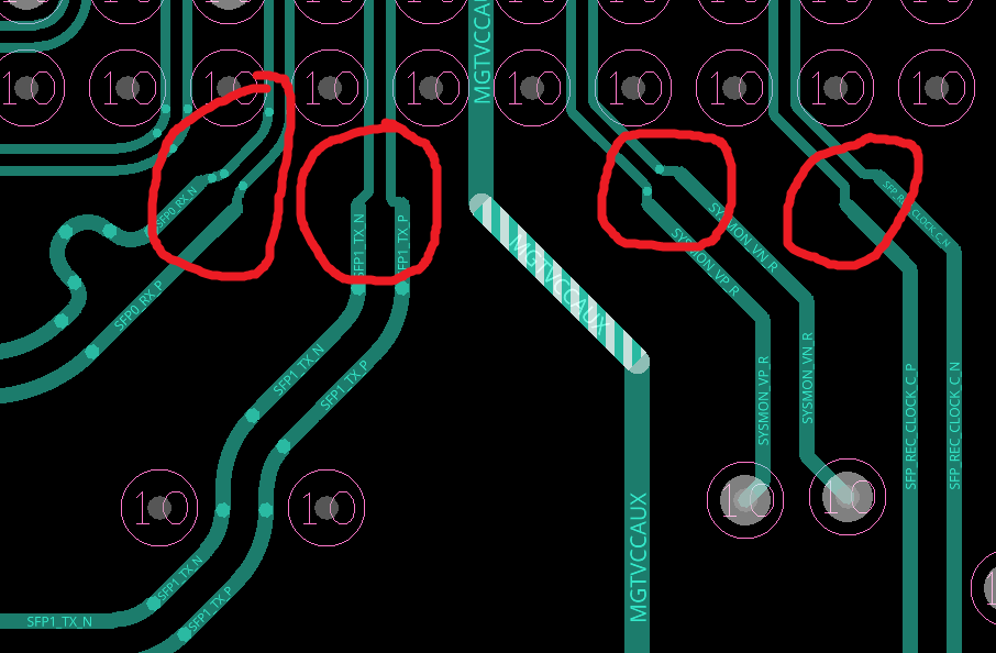
Here is an example from the aforementioned eval board, with the sudden trace gap-changes circled in red.

enter image description here

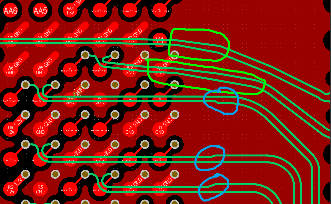
Here is an example of my board, with sudden changes marked in blue and the gradual changes marked in green.

enter image description here

Could someone please advise on the better strategy for this situation and explain why either the sudden gap (ergo, impedance) change or the gradual gap (impedance) change works better?

\$\endgroup\$
2
  • \$\begingroup\$ I guess tapering the traces will have smaller mismatch, but why not route all of the signals according to your 3mil constraint? \$\endgroup\$
    – ZelmaB
    Commented Nov 10, 2021 at 12:05
  • \$\begingroup\$ @ZelmaB Because I need a 6 mil gap to meet 100 Ω impedance constraint. \$\endgroup\$
    – wisner
    Commented Nov 17, 2021 at 20:53

2 Answers 2

4
\$\begingroup\$

A couple of things first:

  • When you change the gap, you also have to change the trace width to obtain the same impedance.
  • I suppose a gradual adjustment would be ideal, but for every point in this transition area, the trace width and gap have to be such that impedance is alright. It will not lead to a straight fan type pattern, but complicated bent patterns.
  • If you are not willing to properly design this long transition pattern that has the right impedance everywhere, the next best thing is directly jumping from the old width and gap to the new width and gap, which will cause approximately constant impedance. The length of impedance mismatch will be very short and not deter wave propagation that much.

Could someone please advise on the better strategy for this situation and explain why either the sudden gap (ergo, impedance) change or the gradual gap (impedance) change works better?
There is no impedance change if done right. Note how they narrow the trace width in the eval board when going from the two single lines to the tight diff-pair. This is done to get the same impedance before and after the change. They were not motivated to design a gradual change as explained above. So they went for the sudden step change. Apparently, it is good enough in that application.

\$\endgroup\$
5
  • \$\begingroup\$ I'm afraid that the initial 3-ish mil gap under the BGA requires either stack-adjustment or trace-width adjustment that we just don't have :/ But your advice has actually encouraged me to revisit the drawing board. I can manage 3 mil width traces with 6 mil gap if I allow for my trace-to-via distance to be smaller, namely 7.5 mil. (Vias have hole diameter 8 mil and plating diameter [including hole diameter] of 12 mil.) Do you think these multi-gigabit traces being only 7.5 mil away from the vias (as opposed to the roughly 9 mil now) would create non-negligible interference? \$\endgroup\$
    – wisner
    Commented Nov 18, 2021 at 5:29
  • \$\begingroup\$ @wisner I can't completely follow tbh. if you set the diff pair to the smallest dimensions allowed by your design rules, it would give you maximum clearance to the vias. Via clearance should be at least 2 trace widths IMO. If this is not possible, you should route only 1 trace between vias and the second trace through another gap. Outside the via forest, go wider to something that will promise good yields. Sorry if I didn't address your question. \$\endgroup\$
    – tobalt
    Commented Nov 18, 2021 at 6:56
  • \$\begingroup\$ The gist of my question was, like, if my via annular ring to trace distance were changed from 9 mil to 7.5 mil, do you think that would create a lot of interference at high speeds? \$\endgroup\$
    – wisner
    Commented Nov 18, 2021 at 8:46
  • 2
    \$\begingroup\$ @wisner Depends also on the dielectric thickness. At 4 mil dielectric, a 7.5 mil gap (during a short run of the trace) is probably ok. At higher dielectric thickness, you want more clearance. But its also important that the proximity is short. Nearby component pins are also close and no problem. So I would say 7.5 mil gap is likely fine, especially for dielectric thickness if 4 mil and below. \$\endgroup\$
    – tobalt
    Commented Nov 19, 2021 at 5:22
  • \$\begingroup\$ This is the best news I've heard all week! Thank you so much for your advice, @tobalt <3 \$\endgroup\$
    – wisner
    Commented Nov 19, 2021 at 16:51
4
\$\begingroup\$

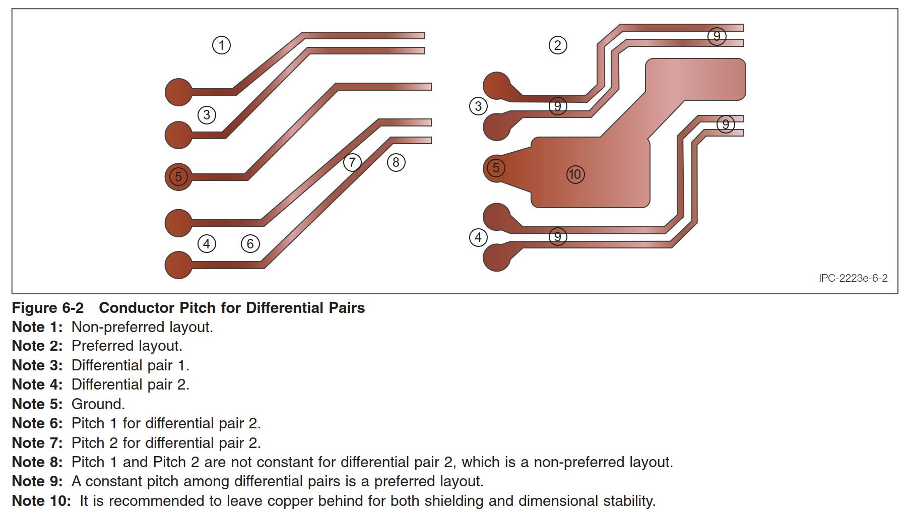
More of a reference than an answer, but, According to IPC-2223E (Sectional Design Standard for Flexible/Rigid-Flexible Printed Boards)

"The conductor pitch for differential pairs used for controlled impedance should be kept constant along the length of the conductor to avoid unwanted signal noise / signal mismatch."

I expect this is generally applicable, rather than just being good-practice for flexi-rigid PCBs.

Conductor Pitch for Differential Pairs

\$\endgroup\$
1
  • \$\begingroup\$ Thank you. I supposed I should have been more specific. A 6 mil gap is required for 100 Ω impedance, but this 6 mil gap does not fit under the BGA. Therefore, I try to use the map possible gap (3-4.5ish mil) under the BGA, then transition to the 6 mil after leaving the BGA area. Do you think in this case there should still be a single 3 => 6 mil transition point? \$\endgroup\$
    – wisner
    Commented Nov 17, 2021 at 20:55

Your Answer

By clicking “Post Your Answer”, you agree to our terms of service and acknowledge you have read our privacy policy.

Not the answer you're looking for? Browse other questions tagged or ask your own question.