5
\$\begingroup\$

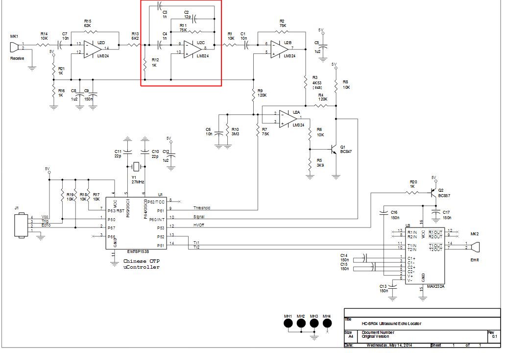
I'm trying to follow along with this blog post reverse engineering the HC-SR04 ultrasonic distance sensor.

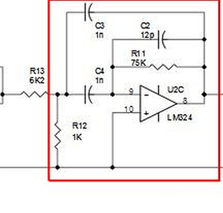
The signal from the receiving transducer is amplified, filtered, and then amplified again.

On the filter, there is a 1 nF cap C4 between the signal and inverting input which I believe is a DC block. There is a second 1 nF cap C3 between the signal and op amp output.

What is the purpose of C3?

The expected signal frequency is 40 kHz.

enter image description here

\$\endgroup\$
2
  • \$\begingroup\$ The shown parts values give a bandpass center frequency of app. fo=19.8 kHz. \$\endgroup\$
    – LvW
    Commented Nov 13, 2021 at 10:08
  • \$\begingroup\$ Why did you think it was 40kHz? \$\endgroup\$
    – D.A.S.
    Commented Nov 13, 2021 at 17:31

4 Answers 4

6
\$\begingroup\$

enter image description here

What is the purpose of C3?

(corrected) Pardon my poor engineeringlish.

I meant Negative Inductance not -L. L is always a positive interger, with positive reactance, while C is a negative reactance, unless used in an impedance converter with feedback.
(so always think in terms of impedance)

C4 is an active inductor or negative capacitor as the negative impedance converter (NIC) while C3 is the active capacitor or negative inductor using negative feedback as an integrator by subtracting its response from the input 820 ohm source impedance. (1k // 6k2) While C2 has very little effect and C4 in series with C3 are equivalent to a passive L//C to virtual AC grounds. (Vin- and Vout) The NIC converts the series C3:C4 notch filter into a BPF using NIC negative feedback via Vin-. (I hope this is clear)

C2 is a weak integrator pole 2 orders of magnitude in f above the BPF, just before the possible GBW limits to normalize the filter variance with IC's having tolerances on a 5~10 MHz GBW or so as to reduce the peak gain variance yet drop it by a fixed amount 3dB. It could improve phase margin on IC's with << 60 deg. that is my hunch.
enter image description here

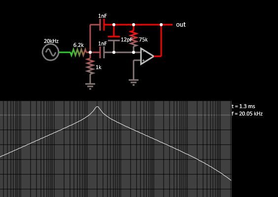
The actual frequency is about 20 kHz with a gain of 12 dB. It is mainly a 2nd order LC parallel resonant filter with some R ratio gain. The 12 pF reduces the Q peaking from 15 dB to 12 dB.

The GBW must be at least 4 MHz and preferably 10 MHz minimum from my RoT (Rule of Thumb).

GBW = Qmax^2 * Av * fo= 64 * 3.3 * 20 kHz

If we had to use an inductor, it would be quite large in physical size to achieve a low ESR <= 10 mohm and 50x times the cost of a cap, roughly. enter image description here
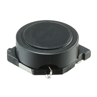
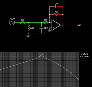
ref This is a rough approximation of a similar LC filter.
enter image description here

This does not mean you can pass 10 Amps thru the Inductance "C4". Something might explode. (LOL)

But the Op Amp draws current from supply to do the same as the inductor, except this is an inverting NIC. or INIC.

\$\endgroup\$
14
  • 1
    \$\begingroup\$ @Tony Stewart, with all respect, I cannot follow your explanation. Of course, you can replace the shown active RC circuit with a corresponding LC circuit. Such a step is always possible. However, how can you say that "C3 is an active inductor"? In the original circuit the capacitor C3 provides a LOW-pass function to the circuit (and C4 acts as a highpass). But in the LC equivalent, the inductor is responsible for the HIGH-pass properties (and it attenuates low frequencies). So the capacitor C3 does exactly the opposite as mentioned by you. \$\endgroup\$
    – LvW
    Commented Nov 12, 2021 at 10:10
  • 1
    \$\begingroup\$ But where do you see an impedance converter NIC? More than that, it is the input impedance of the whole NIC circuit (and NOT the capacitor alone) which can behave like a lossy inductance. I think, such a view has nothing to do with the circuit under question. \$\endgroup\$
    – LvW
    Commented Nov 12, 2021 at 14:16
  • 1
    \$\begingroup\$ With respect to the corrected version of the above answer: The reference to a negative impedance converter (NIC) is not correct. A short look into the linked document reveals that the bandpass circuit under discussion has no relation to an NIC block. \$\endgroup\$
    – LvW
    Commented Nov 12, 2021 at 15:17
  • 1
    \$\begingroup\$ More than that: I can read that " C4 is an active inductor or negative capacitor" and "C3 is the active capacitor or negative inductor ". Such a claim needs an explanation. I wonder how a negative capacitor can have a frequency response like an inductor? \$\endgroup\$
    – LvW
    Commented Nov 12, 2021 at 17:27
  • 1
    \$\begingroup\$ Quote: "C4 is an active inductor or negative capacitor". Again I ask you: How can an active inductor be identical to a negative capacitor? Does this mean that the impedance jwL is equal to (-1/jwC=j/wC) ? No - of course, not! When you read again the third comment above, you will see that I know something about VNIC and INIC. But the main point is: The whole story about the NIC has nothing to do with the original question and the bandpass circuit under discussion. Why did you even bring that up? \$\endgroup\$
    – LvW
    Commented Nov 13, 2021 at 9:10
5
\$\begingroup\$

Welcome to EE.SE.

The block highlighted in red is an active bandpass filter, which C3 and C4 are part of. See https://www.electronics-tutorials.ws/filter/filter_7.html under Infinite Gain Multiple Feedback Active Filter. Presumably it is tuned to 40 kHz. I haven't checked but you are welcome to plug the component values into the formula given in the link.

C2 rolls off the gain at high frequency (>> 40 kHz) to improve the stability of the filter i.e. prevent it oscillating.

\$\endgroup\$
2
  • \$\begingroup\$ The filter is stable - even without C2. It is the only purpose of C2 to increase the damping for very large frequencies. C2 adds a lowpass characteristic to the bandpass (3rd-order damping for high frequencies far above the bandpass center frequency.) \$\endgroup\$
    – LvW
    Commented Nov 12, 2021 at 11:14
  • \$\begingroup\$ The center frequency of the given circuit is app. at fo=19.8 kHz \$\endgroup\$
    – LvW
    Commented Nov 13, 2021 at 10:06
3
\$\begingroup\$

That filter topology is called a narrow-band multiple-feedback (MFB) band-pass filter.

C3 and C4 are both part of the band pass filter and define the pass band frequency range.

\$\endgroup\$
2
\$\begingroup\$

This is one of the known methods to improve the damping characteristics of a second-order bandpass.

  • With the exception of C2, all the other parts resemble the well-known second-order bandpass in multi-feedback-topology.

  • The additional capacitor C2 adds an additional lowpass function to the circuit with a pole at app. fp=180 kHz [wp=1/T=1/(12p*75k)]. This effect can be seen in the BODE diagram: The rising slope is +20dB/dec whereas the falling slope of the magnitude approaches -40dB/dec.

\$\endgroup\$

Your Answer

By clicking “Post Your Answer”, you agree to our terms of service and acknowledge you have read our privacy policy.

Not the answer you're looking for? Browse other questions tagged or ask your own question.