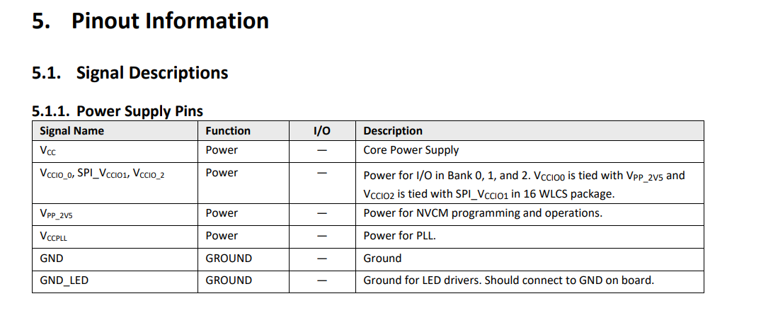
I'm having trouble understanding the structure of FPGA datasheets. From what I can tell, there is usually a table of "Signals Descriptions" with the pin names and their function, but I don't see any indication of the pin number. See example below, from Lattice "iCE40" datasheet.
How are the actual pin numbers determined? Is this defined elsewhere? Is it decided only by the VHDL/Verilog code (and if so, can any number be any signal)?

