4
\$\begingroup\$

enter image description here

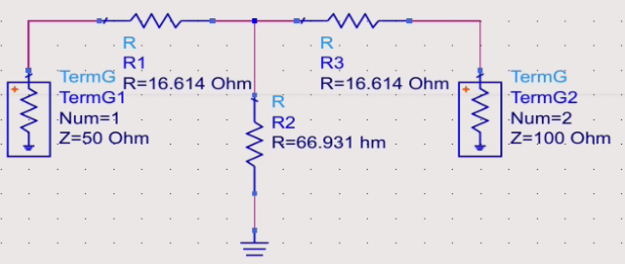
The attenuator given in the figure is a 6 dB attenuator when both port 1 and 2 have a reference impedance of 50 Ω.

Then, their S-parameter matrix (when port 1 and 2 have 50 Ω reference impedance) would look like $$S=\begin{bmatrix}S_{11} && S_{12} \\ S_{21} && S_{22}\end{bmatrix}=\begin{bmatrix}0 && 0.5 \\ 0.5 && 0\end{bmatrix}$$

Now, I changed the reference impedance of port 2 to 100 Ω as shown in the figure. Based on some of readings from Pozar's microwave textbook, the following is what I thought it should be:

enter image description here

Let $$Z_{o1}=50 \Omega $$ and $$Z_{o2}=100 \Omega$$, respectively. Then $$Z_{in,1} = R_1 + R_2 \parallel (R_1 + Z_{o2})$$ $$Z_{in,2} = R_1 + R_2 \parallel (R_1 + Z_{o1})$$ $$\Gamma_S = \frac{Z_{o1} - Z_{in,1}}{Z_{o1} + Z_{in,1}} = \frac{V_1^+}{V_1^-}$$ $$\Gamma_L = \frac{Z_{o2} - Z_{in,2}}{Z_{o2} + Z_{in,2}} = \frac{V_2^+}{V_2^-}$$

Then we have: $$V_1^- = S_{11}V_1^+ + S_{12}V_2^+$$ $$V_2^- = S_{21}V_1^+ + S_{22}V_2^+$$ Since $$\Gamma_L = \frac{V_2^+}{V_2^-} $$, we have: $$V_2^- = S_{21}V_1^+ + S_{22}\Gamma_LV_2^-$$ $$S_{21}'=\frac{V_2^-}{V_1^+} = \frac{S_{21}}{1-S_{22}\Gamma_L}$$ and $$\Gamma_S = \frac{V_1^+}{V_1^-}$$ $$V_1^- = S_{11}V_1^+ + S_{12}V_2^+ = S_{11}\Gamma_SV_1^- + S_{12}V_2^+ $$ $$V_1^- = \frac{S_{12}}{1-S_{11}\Gamma_S}\cdot V_2^+ $$ $$V_2^- = S_{21}\Gamma_SV_1^- + S_{22}V_2^+ = \left(\frac{S_{21}\Gamma_SS_{12}}{1-S_{11}\Gamma_S} + S_{22}\right)V_2^+$$ $$S_{22}'=\frac{V_2^-}{V_2^+}=\frac{S_{21}\Gamma_SS_{12}}{1-S_{11}\Gamma_S} + S_{22}$$

Based on the above computation, I was getting $$S_{11}'= -21.54\text{ dB,} \quad \quad S_{21}'= -6\text{ dB} \quad \text{, and}\quad S_{22}'=-33.543\text{ dB}$$

Compared to the ADS simulation results, S_{11}' is correct but S_{22}' and S_{21}' are wildly wrong. The simulation results say: $$S_{11}'= -21.54\text{ dB,} \quad \quad S_{21}'= -6.512\text{ dB} \quad \text{, and}\quad S_{22}'=-9.542\text{ dB}$$

In addition, intuitively speaking, I thought S_{22}' should be $$S_{22}' = \frac{Z_{in,2} - Z_{o2}}{Z_{in,2} + Z_{o2}} \neq \frac{S_{21}\Gamma_SS_{12}}{1-S_{11}\Gamma_S} + S_{22}$$ For this problem, when I use the middle equation I get the correct S_{22}.

In summary, I would like to know

Q1. How to correctly compute \$S_{21}\$ in this scenario where the reference impedances of port 1 and 2 are different

Q2. If the reference impedances of port 1 and 2 are different, which equation is correct for \$S_{22}'\$?

I spent more than 6 hours today but couldn't come up with the right answer. I would sincerely appreciate it if anyone can answer my question above.

Thanks!

\$\endgroup\$

2 Answers 2

2
\$\begingroup\$

In general, assuming that the reference impedances in consideration are real, S-Parameters have the following definition: $$\frac{V_{r1}}{\sqrt{Z_1}} = S_{11}\frac{V_{i1}}{\sqrt{Z_1}}+S_{12}\frac{V_{i2}}{\sqrt{Z_2}}$$ $$\frac{V_{r2}}{\sqrt{Z_2}} = S_{21}\frac{V_{i1}}{\sqrt{Z_1}}+S_{22}\frac{V_{i2}}{\sqrt{Z_2}}$$ Here, \$Z_1, Z_2\$ is reference impedance at port 1 and 2 respectively.
If reference impedance is real, then the power waves can be viewed as travelling voltage waves scaled by the appropriate reference impedance. Thus, $$S_{11} = \frac{V_{r1}}{V_{i1}}\vert_{V_{i2}=0}$$ $$S_{21} = \sqrt{\frac{Z_1}{Z_2}}\frac{V_{r2}}{V_{i1}}\vert_{V_{i2}=0}$$

So, for your example, $$ Z_{in1} = 16.641+ \frac{116.641 \cdot 66.931}{116.641 + 66.931} = 59.138$$ $$S_{11} = \frac{V_{r1}}{V_{i1}} = \Gamma_1 = 20*log10(\frac{59.138-50}{59.138-50}) = -21.54dB$$ Assuming, voltage at input node is \$V_x\$ and output node is \$V_y\$: $$V_{x} = V_{i1}+V_{r1} = (1+\Gamma_1)V_{i1} = 1.083V_{i1}$$ $$V_{y} = V_{i2}+V_{r2} = V_{r2}$$ Because of matched load, there is no incident wave at node 2. $$V_{y} = V_{r2} = (V_x - \frac{V_x}{59.138}.16.614)\frac{100}{100+16.614} = 0.616V_x$$ $$\frac{V_{r2}}{V_{i1}} = 0.616\cdot1.083 = 0.667$$ $$S_{21} = \sqrt{\frac{50}{100}}\cdot 0.667 = -6.52dB$$ $$S_{22} = \Gamma_2 = \lvert{\frac{50-100}{50+100}}\rvert = -9.54dB$$ This is same as what the simulator shows you.

\$\endgroup\$
8
  • \$\begingroup\$ Thanks a lot for the detailed comment. I have two extra questions regarding this: Q1. I'm very confused about S-parameter definition. For instance, S11 is defined as the ratio of reflected voltage wave to the incident voltage wave at port 1 when the incident voltage wave at port 2 is 0. However, we do know that Zo2 (reference impedance of port2 = 100 ohm) is not equal to the input impedance looking from port 2 (50 ohm). In this case, regardless of the port 2 reference impedance, do we just force the incident voltage wave at port 2 is 0? \$\endgroup\$
    – Emm386
    Commented Dec 6, 2021 at 3:40
  • \$\begingroup\$ Q2: From Pozar's textbook, Gamma_out is defined as s22+(S12*S21*Gs)/(1-S11*Gs), where Gs is the reflection coefficient looking into port 1. If I use this equation, I get different S22 from what you have. If you can, could you point out if I miss anything here? \$\endgroup\$
    – Emm386
    Commented Dec 6, 2021 at 3:42
  • \$\begingroup\$ @Emm386 Regarding the first question, the reflected wave at port 2 \$V_{r2}\$ when "reaches" port 2 sees an impedance equal to the reference impedance and so there is no reflection \$V_{i2}\$ back from that port. This is the reason we keep the port 2 terminated at the reference impedance. \$\endgroup\$
    – sarthak
    Commented Dec 6, 2021 at 5:53
  • \$\begingroup\$ Q2:, Gs = 0 since Zs is same as Zo1 and so Gamma_out = S22, which is -9.54dB as calculated above. \$\endgroup\$
    – sarthak
    Commented Dec 6, 2021 at 5:55
  • 1
    \$\begingroup\$ Thank you so much for your comment. There was big misconception that I had about the calculation of reflection coefficients, and you explained in very clear way. My questions are all solved. Thank you! \$\endgroup\$
    – Emm386
    Commented Dec 7, 2021 at 19:41
3
\$\begingroup\$

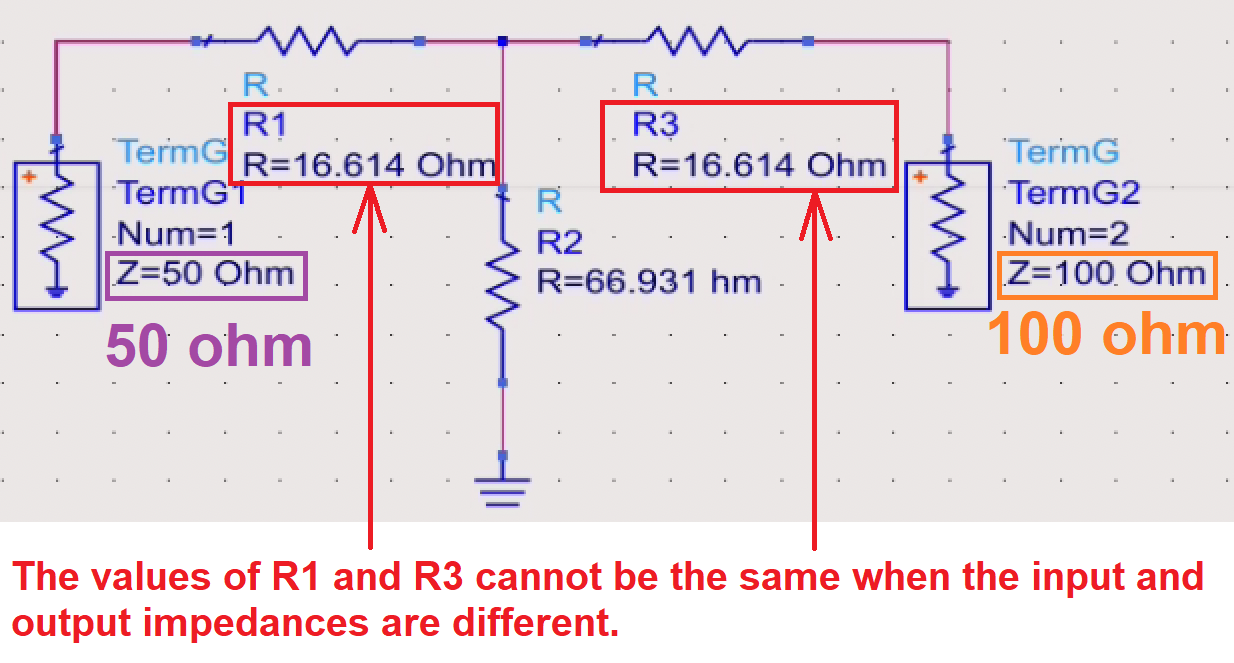
You show this in your question and, it cannot be correct: -

enter image description here

So, moving on from this despite your downvote...

How to correctly compute S_{21} in this scenario where reference impedance of port 1 and 2 are different

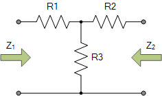
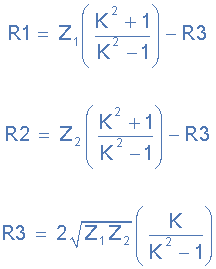
Why don't you use the standard formulas for a T attenuator: -

enter image description here

enter image description here

Where: K is the impedance factor from below, and Z1 is the larger of the source/load impedances and Z2 is the smaller of the source/load impedances.

enter image description here

Unfortunately, the K formula is incorrect but, I've amended that in my addendum at the bottom of this answer.

Images stolen from this electronics-tutorials.

I might add that the derivations are a little bit tricky if you are thinking of doing them yourself.

If the reference impedance of port 1 and 2 are different, which equation is correct for S22'?

If you use the formulas above correctly (noting the error I found) then S22 will be the required output impedance for the load.


Addendum that corrects the K formula

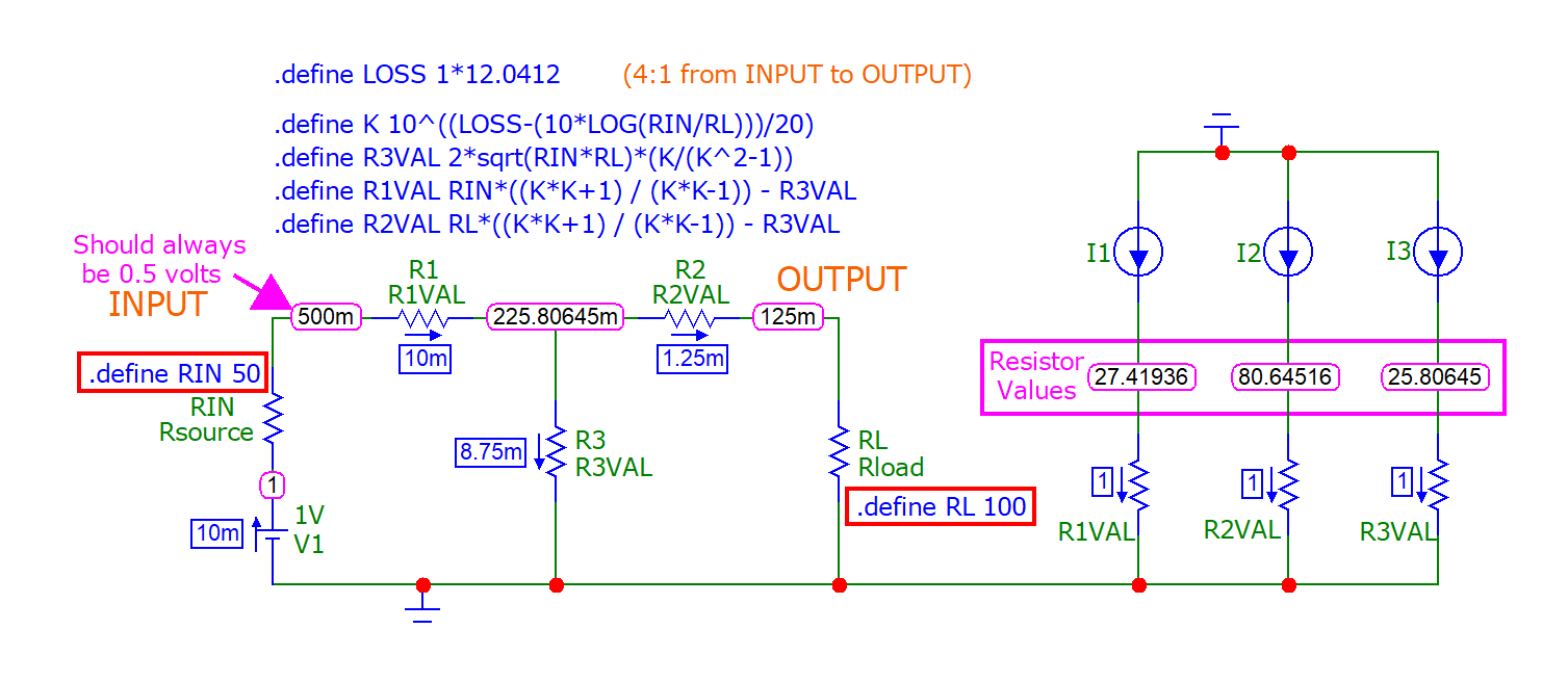
Micro-cap set-up for a 4:1 attenuation (12.0412 dB) with RIN = 50 Ω and RL = 100 Ω: -

enter image description here

So, with a 1 volt source having a 50 Ω source resistance, the voltage appearing at the left of R1 is, as expected, 0.5 volts. And, with an attenuation of 4:1 (12.0412 dB), as expected, the output voltage is 125 mV. The website having the original pictures neglected the \$10\cdot LOG(RIN/RL)\$ term when calculating K. For equal input and output resistors and 4:1 dB attenuation you get this: -

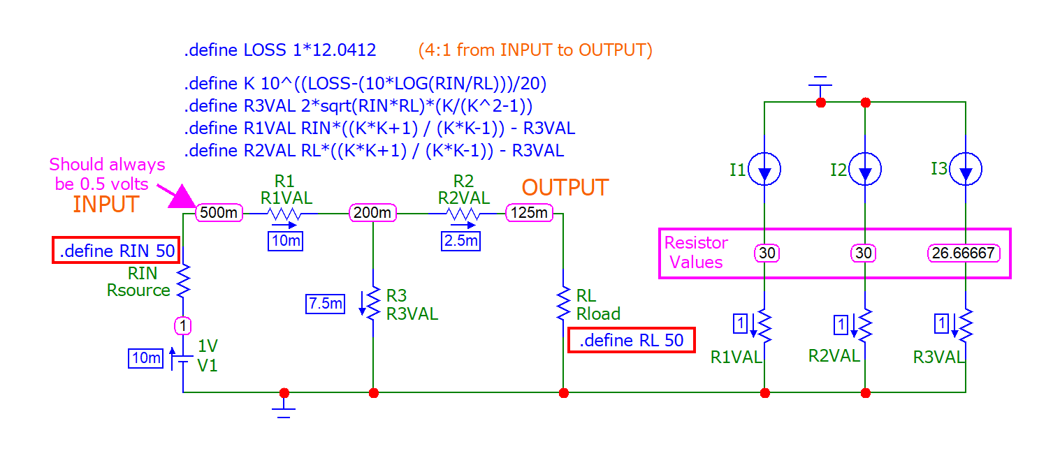
enter image description here

As you can probably see R1 = R2 = 30 Ω and, R3 = 26.6667 Ω. If you crunched the numbers (do you really need to given that micro-cap is boss), you'll get exactly what is written on the tin.

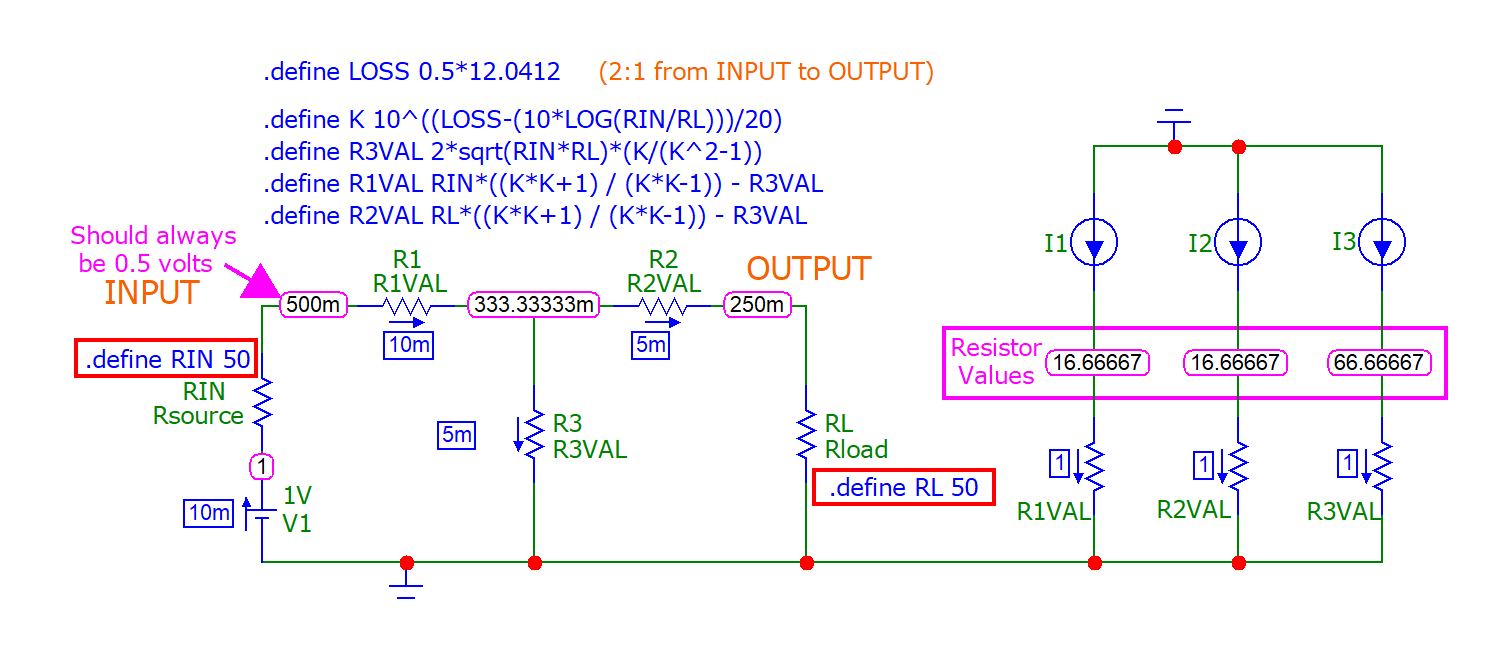
For 2:1 attenuation: -

enter image description here

Hey, it's given me something to do on a bleak Sunday afternoon!

\$\endgroup\$
7
  • \$\begingroup\$ thanks for your comment, but unfortunately this is not what I was looking for. My question was specifically about how to compute "S21" for general 2-port network when the reference impedance of port 1 and 2 are different. \$\endgroup\$
    – Emm386
    Commented Dec 4, 2021 at 19:27
  • \$\begingroup\$ Plus, I've used those equations above and I'm getting -8 dB for 'K', which is different from -6.512 dB that ADS reports to me \$\endgroup\$
    – Emm386
    Commented Dec 4, 2021 at 19:29
  • \$\begingroup\$ Well, its up to you but I'd be thinking about posting those calculations. Also, my comment is an answer. If you don't see it as an answer (as per your first comment above) then I have to say that I do not know what you mean. As far as I'm concerned, I have answered your question. \$\endgroup\$
    – Andy aka
    Commented Dec 4, 2021 at 20:24
  • \$\begingroup\$ @Emm386 I've added several more layers to this and recognized that the website that gave the original formulas have an error (as do all the websites on tapered pad attenuators). You still may believe that I'm not helping of course but, you ought to review what you are asking and look at it from the perspective of somebody reading your question. I appear to be the only one giving you support on this so please do consider more what I'm saying and look at the amendments to my answer. \$\endgroup\$
    – Andy aka
    Commented Dec 5, 2021 at 17:54
  • \$\begingroup\$ Thanks Andy for putting lots of effort into this and giving me extra information during Sunday afternoon. I really appreciate your extra information, however, this is not what I was asking. there are two reasons. One is that I was asking specifically for "mathematical" expression for S21. In this case, 'K' simply represents the voltage gain which is slightly different from S21. the definition of S21 is the ratio of "reflected power wave of port 2" to "incident power wave of port 1". In this context, 'K' is rather a sum of incident and reflected power wave over reference impedance. \$\endgroup\$
    – Emm386
    Commented Dec 6, 2021 at 3:59

Your Answer

By clicking “Post Your Answer”, you agree to our terms of service and acknowledge you have read our privacy policy.

Not the answer you're looking for? Browse other questions tagged or ask your own question.