1
\$\begingroup\$

I have been reading about transistor biasing to counteract inaccuracies in transistor manufacture, add stability etc.

One circuit I can't see the benefit in, which is diagrammed in the datasheet for the PEMD17, has a resistor between the emitter and base. Of all of the standard biasing configurations I've read about, I've not read about this one. It looks just like a voltage divider on the input signal.

From the datasheet, I would expect to ground pin 1, apply a signal at 2 to control a load at pin 6. The R2 seems to have no benefit other than to alter the base input.

The following diagram shows how I would expect to use the circuit. Is that application incorrect?

schematic

simulate this circuit – Schematic created using CircuitLab

\$\endgroup\$
5
  • 1
    \$\begingroup\$ A feedback resistor would couple an output to an input. Here, R2 couples ground to the input. Ground is not an output. There is no signal on ground. Ground is always 0 V (by definition). If there is a voltage (signal) on ground, it is not ground anymore. \$\endgroup\$ Commented Dec 8, 2021 at 15:23
  • \$\begingroup\$ So what is R2's job? I appreciate JRE's answer but I suspect there must be more to it. \$\endgroup\$
    – J Collins
    Commented Dec 8, 2021 at 15:29
  • \$\begingroup\$ but I suspect there must be more to it. Why? JRE's answer is 100% correct. I will also claim that 95 out of 100 circuit designers will leave out R2, assuming that the input (left of R1) is pulled to ground when the transistor Q1 needs to be off. If the signal controlling the transistor comes from any microcontroller or logic gate, that will be the case and R2 is not needed at all. \$\endgroup\$ Commented Dec 8, 2021 at 15:36
  • \$\begingroup\$ Also: there is no mention in the datasheet of the PEMD17 that it is desigend to be used as it is in your schematic. In your circuit, there might be no need for R2 if the input voltages are chosen correctly. The PEMD17 might be designed for a very different use of the transistors. \$\endgroup\$ Commented Dec 8, 2021 at 15:39
  • \$\begingroup\$ My application is a simple high-side switch for a battery powered device's 'key', that needs to use 3.3V or 5V logic to pull a wire to the battery voltage (up to 50V). A NPN/PNP combination will work, the extra resistors just threw me. \$\endgroup\$
    – J Collins
    Commented Dec 8, 2021 at 16:17

3 Answers 3

7
\$\begingroup\$

R2 is there so that the circuit is in a defined state when there's no signal on R1.

If you have a high or a low on the input at R1, then the circuit works like you expect - it switches the load on when the input is high and off when it is low.

If R1 is left open (remove the signal generator from your diagram,) then stray voltages and currents may appear on the base of Q1. That can randomly turn your load on or off - or somewhere inbetween.

R2 pulls the base of Q1 down to zero volts so that the load is off when there's no input on R1.


Consider a microcontroller driving a small motor through a transistor.

At power on, the output pins of many modern microcontrollers can be undefined - they are high impedance (open) until your code says to set them to output mode at a particular level. Until your code executes, the output is floating. If there's any electrical noise in the vicinity, enough current may flow through the base of the transistor to cause the motor to run.

If you have a pull down on the base of the transistor, then the stray voltages will have to be very substantial to make the motor run. That pull down makes the system stable during start up.

\$\endgroup\$
3
  • \$\begingroup\$ That is an interesting application, though it would suggest there is no relevance to the bias ratio of the resistors as discussed in the datasheet. It seems to be quite specific about their ratios. \$\endgroup\$
    – J Collins
    Commented Dec 8, 2021 at 15:23
  • 1
    \$\begingroup\$ That's what it is for. The datasheet says that those pre-biased transistors are for switching applications. They specify the ratios so that you know what you are getting. You need to know so that you can figure total circuit current consumption in low power (battery powered) devices. \$\endgroup\$
    – JRE
    Commented Dec 8, 2021 at 15:31
  • \$\begingroup\$ It is a surprising need, but I'm definitely satisfied that it is the right answer..! Marked as such. \$\endgroup\$
    – J Collins
    Commented Dec 8, 2021 at 16:19
1
\$\begingroup\$

The problem

When current driven (via a base resistor), a BJ transistor is very sensitive and amplifies small leakage currents. The reason for this behaviour is that the resistance of the PN junction is non-linear. In the beginning it is very high, and at a negligible current the voltage across it rises to several hundred millivolts.

The remedy

Therefore, the initial high input resistance must be lowered. This means that the transistor must be controlled by voltage (via a low-resistance voltage divider).

Intuitive explanation

Transistor "microammeter"

The base-emitter junction can be thought as a "sensitive microammeter". For example, if the collector current needed to saturate the transistor is 1 mA and β = 100, it would be "10 μA ammeter" with 70 kΩ internal resistance and about 700mV voltage drop. Then 930 kΩ leakage resistance will be enough to saturate the transistor.

Actually, the two resistances form a high-resistance voltage divider with a gain of Rbe/(Rb + Rbe). It "produces" 700 mV base voltage that is enough to saturate the transistor.
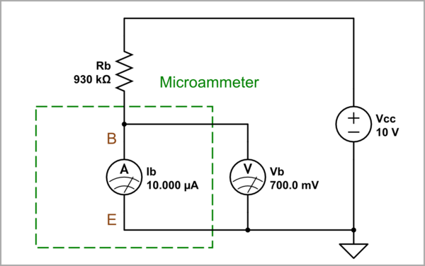
schematic

simulate this circuit – Schematic created using CircuitLab

Transistor "milliammeter"

We can decrease the "microammeter" sensitivity by shunting it e.g. with a 1 kΩ resistor. Then to saturate the transistor, Rb should be less than 13 kΩ.

Now the two resistances Rb and the additional Rbe form a low-resistance voltage divider with the same gain as above. It "produces" 700 mV base voltage that is enough to saturate the transistor.
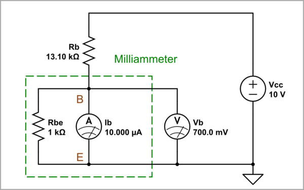
schematic

simulate this circuit

Resistance discriminator

So the last circuit (with a 13 kΩ base resistor and a shunting 1 kΩ resistor between the base and emitter) clearly differentiates the two values ​​of Rb. Assuming it is driven by an open-collector PNP transistor, it means that the first value (> 930 kΩ corresponds to the OFF state of the transistor, and the second (< 13 kΩ) to the ON state.

Conclusion

The role of the shunt resistor R2 connected between the base and the emitter is to decrease the initial high input resistance when Vbe < 700 mV. As a result, the transistor can be controlled only by low base resistance Rb (significant input current), and will not react to small leakage currents.

\$\endgroup\$
0
\$\begingroup\$

Quote J. Collins: "So what is R2's job? I appreciate JRE's answer but I suspect there must be more to it"

Yes - indeed, I think there is an additional argument for R2:

  • We know that a minimum voltage Vbe is needed to bring the BJT into saturation (switching application). Such a minimum value for Vbe is needed to allow a collector current Ic which can fulfill the saturation condition (Vce<Vbe)

  • Equation: Vbe=V1-(I2+Ib)R1=V1-(I2+Ic/B)R1. (V1: on-level, I2: current through R2)

  • As we can see, any uncertainty in B (large tolerances)will have a small influence on the required Vbe value as long as I2>>Ib.

  • More than that, the actual Ib value depends also on the Vce value (C-B junction forward biased)

Without R2 (I2=0) the uncertainty/tolerance of B goes directly into the Vbe level. The price we have to pay for this advantage could be a larger value for the input switching level V1 (if R1 remains constant).

\$\endgroup\$

Your Answer

By clicking “Post Your Answer”, you agree to our terms of service and acknowledge you have read our privacy policy.

Not the answer you're looking for? Browse other questions tagged or ask your own question.