2
\$\begingroup\$

I'm trying to achieve a variable voltage supply where the voltage can be tuned by a DAC. The DAC is limited to ~3.3 V, but the design goal for the resulting voltage supply is V_out between 0 and 15 V and current up to 500 mA.

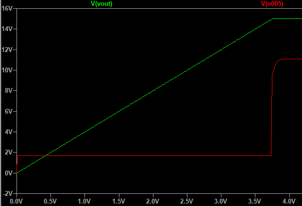
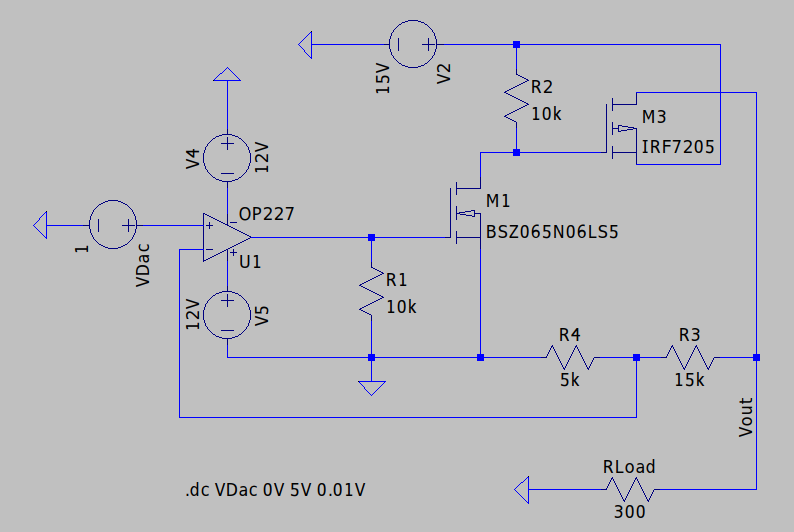
My current design consists of a driving a P-channel MOSFET with a N-channel MOSFET, which is controlled by an OpAmp. (The negative side of the load has to be connected to GND directly and so I cannot use a N-channel MOSFET directly and put it in the GND-path. Hence I used a P-channel MOSFET.) When I simulate this circuit in LTSpice I get the desired output, independent of the load (which I have modeled with a simple resistor here, and the DAC as a sweep between 0 and 5 V).

enter image description here Green: Output voltage. Red: Voltage at the OpAmp output. X Axis: Voltage of the DAC

Now I have the following questions:

  1. While it seems to work in LTSpice, I failed to reproduce the behavior with real components (OPA202, N-MOSFET ZVN4106FTA, P-MOSFET PJA3441). Instead, I only can get it to switch between 0 and 12 V, with no real linear behavior. I tried to use models with similar values in LTSpice - but is there anything in particular that I need to pay attention when choosing MOSFETs for this circuit, besides the max Vds, Vgs threshold and max. Isd?

  2. Because the resistance of both MOSFETs is not linear with the Vgs, the voltage range for Vgs is extremely small and hence the voltage produced by the OpAmp needs to move within very tight boundaries (in the simulation above, the red line showing the OpAmp output voltage is almost always between 1.68 and 1.69 V for the whole range). I'm wondering: isn't this design prone for noise and instabilities, because there is no real stable operating point for the OpAmp? Do you have a suggestion for a good, maybe more linear alternative?

\$\endgroup\$
8
  • 1
    \$\begingroup\$ There's just way too much gain in this circuit. Why don't you leave out M1? You'd just have to connect the OpAmp's output directly to M3's gate (and add a gate protection zener). And of course you'll need to run your OpAmp with +15V instead of +12V. \$\endgroup\$ Dec 27, 2021 at 18:57
  • 1
    \$\begingroup\$ Controlling the output voltage of a DCDC converter or a linear regulator with a DAC takes 3 resistors. Why not use a ready made IC instead of the (much harder) task of designing a regulator from scratch? \$\endgroup\$ Dec 27, 2021 at 19:08
  • 1
    \$\begingroup\$ dc analysis can be quite misleading and doesn't spot instability very well. To this end, what @JonathanS. said \$\endgroup\$
    – tobalt
    Dec 27, 2021 at 19:24
  • \$\begingroup\$ You can use a "weird trick" to quantify and optimize loop stability in LTSpice: Apply an AC stimulus to your circuit somewhere (preferably at VDac) and perform an AC analysis. Then plot the expression "V(IN-)/V(IN+,IN-)" where IN+ and IN- are the inputs of your OpAmp. The resulting graph is the loop gain of the circuit. You can spot any instabilities directly in this graph by reading off the phase and gain margins. You should have at least 45° phase margin and 10dB gain margin. If not, lower the circuit's gain. If you want to remove M1, you'll have to swap the OpAmp's + and - inputs. \$\endgroup\$ Dec 27, 2021 at 20:38
  • \$\begingroup\$ Thanks for the feedback. Do you have any recommendations for ready made voltage regulator ICs to be controlled by a DAC, where I can set the full range from 0 - 15 V (or higher)? Otherwise I guess increasing the supply voltage of the OpAmp and connecting directly to the P-Mosfet might be a good alternative... \$\endgroup\$
    – mrspl
    Dec 27, 2021 at 23:06

1 Answer 1

5
\$\begingroup\$

OpAmps are generally difference amplifiers with super high gain and a built-in low-pass. They become unstable if they still have gain at a frequency where the overall feedback path has 180° phase shift or more. (This is the Barkhausen stability criterion.) Their gain is therefore set so that it falls off to 0dB just before this "instability frequency" (the point with 0° phase margin). If you add external gain, you also increase the gain at this critical frequency. As soon as it reaches 0dB or more, the circuit will oscillate. You can see this in figure 18 of the OP227's datasheet: If you add 6dB external gain (2x amplification), it'll be unstable because the OpAmp will still have gain at the point where it has 0° phase margin (at ~20MHz).

Therefore it is a bad idea to add external gain to most OpAmps; they generally need their feedback network to attenuate, not amplify. Some (decompensated) OpAmps aren't even stable as voltage followers; they're only stable at or above a certain overall circuit gain (i.e. a gain of 2 for the LT1028). Given that you have added not only one, but two external common-source gain stages to an OpAmp that's only barely stable as a voltage follower, it's no wonder that your circuit malfunctions.

In general, an OpAmp's feedback path must not have gain (unless you really know what you're doing and have checked that the OpAmp will be stable with that external gain). This doesn't mean you can't add any amplifying stages to the feedback path, though - it's fine as long as the overall gain of the feedback path is 0dB or less. (A 6dB amplification followed by 6dB attenuation would still work, for example.)

In your case, you should probably replace M1/M3 with a single NPN emitter follower. That doesn't have voltage gain and won't impact the stability of your OpAmp. If you need the output voltage to get close to the input voltage, you have to use a rail-to-rail output OpAmp.

\$\endgroup\$
3
  • \$\begingroup\$ Thanks for the detailed explanation. I still have trouble understanding where the gain in the feedback loop is coming from - due to the voltage divider the OpAmp should only ever sees a much smaller voltage? Is the problem that the voltage divider doesn't attenuate at the higher frequencies at which the OpAmp operates and therefore I effectively have gain at these frequencies? \$\endgroup\$
    – mrspl
    Dec 29, 2021 at 12:49
  • 1
    \$\begingroup\$ M1 and M3 each have gain. You have already noticed that when the output voltage of the OpAmp changes a little, the output voltage of the overall circuit changes a lot. That's gain (amplification). In general, if an OpAmp's output voltage changes by an amount X, the feedback voltage may not change by more than X either. The voltage divider does remove some of that additional gain but by far not all of it. The gain of a common-source MOSFET amplifier is also quite unpredictable. (The feedback path is everything between the OpAmp's output and inverting input, including M1/M3). \$\endgroup\$ Dec 29, 2021 at 13:13
  • \$\begingroup\$ Ahh, of course, I have to look for the gain between the OpAmp output and the feedback loop, somehow I was always thinking about the gain between input to the OpAmp and what's coming from the feedback loop. Thanks for the clarification. \$\endgroup\$
    – mrspl
    Dec 29, 2021 at 13:17

Your Answer

By clicking “Post Your Answer”, you agree to our terms of service and acknowledge you have read our privacy policy.

Not the answer you're looking for? Browse other questions tagged or ask your own question.