4
\$\begingroup\$

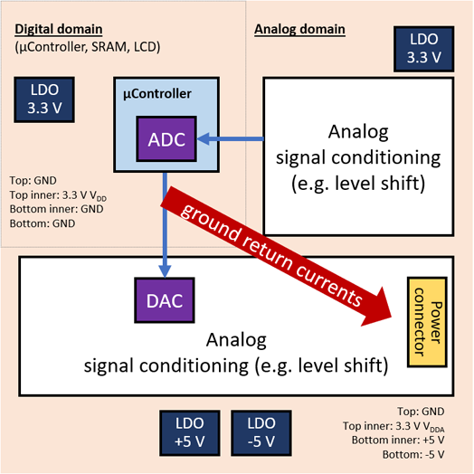
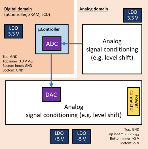
I have the topology as shown in the first picture for an audio application: a digital domain with a µController with integrated 16-bit ADCs, and an analog domain with partially symmetrical supplies and an external 16-bit DAC.

The DAC has the analog and digital grounds combined. The arrows in blue show the analog signal flow to the ADC and the DAC control signals respectively.

enter image description here

I read this well-written solution where a similar question was asked and tried to apply it to my situation. However, I am still unsure if this will work properly because with the ground planes merged, the ground currents from the digital domain will likely choose a direct path straight through the analog domain to my supply connector as shown in the following picture.

enter image description here

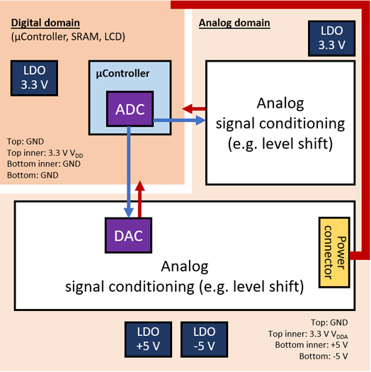
So to aid the return current from the digital domain around the analog domain, I can separate the domains again, add a wide ground trace as shown in the third picture and include some thin ground return wires for my ADC and DAC interconnects. However, that still allows some ground return currents to choose the thinner wires through my analog domains.

enter image description here

I am not clear what to do here to avoid ground currents from the digital domain to cross through the analog part of my topology. So how should this be done properly?

With some effort, I could move the supply connector somewhere between the two domains but what are the alternatives, if any, if I want to leave the connector at the current position? Are there drawbacks if I move my connector between the two domains?

\$\endgroup\$
3
  • \$\begingroup\$ Use isolated DC/DC converters (they are great), or more than one PSU or batteries with grounds connected if components need to communicate. Use a star ground configuration to avoid ground loops. \$\endgroup\$
    – Codebeat
    Commented Dec 28, 2021 at 11:00
  • \$\begingroup\$ Where are the analog connectors on the board? It is important to have all the grounds of all the connectors at the same potential, especially the analog connectors. Is the power supply +5/-5? Is the 3V3 for the micro and other chips derived from analog +5? Is the power supply a SMPS, and if so does it need extra filtering before powering the opamps? (check for HF noise etc). Can you give a datasheet for the micro? (I'm interested in the layout and wiring of the internal ADC). \$\endgroup\$
    – bobflux
    Commented Dec 28, 2021 at 12:16
  • \$\begingroup\$ @bobflux, All LDOs are directly supplied from the power connector. They are not interconnected (e.g. the LDO for the digital 3.3 V is different from the LDO for the analog 3.3 V). The µController is the STM32H745 (BGA version; I am using VREF from this µController for reference purposes). All GND is interconnect, no ground separation. For analog supply, I am using the TPS7A4901DRBR with the corresponding resistor dividers. The LDO for the µController is a TLV76733DRVR. \$\endgroup\$
    – Hansel
    Commented Dec 28, 2021 at 14:42

3 Answers 3

2
\$\begingroup\$

So to aid the return current from the digital domain around the analog domain, I can separate the domains again, add a wide ground trace as shown in the third picture and include some thin ground return wires for my ADC and DAC interconnects.

No, you should use an unbroken ground plane.

I presume your micro is sending some fast digital signals like I2S to your DAC chip. These have corresponding return currents. If they are routed over a split in the ground plane, return current will take the long way around, resulting in a lot more noise.

I've had success with a simple solution: make the current draw of the noisy chip constant. This way, power supply and ground return currents between your micro and the power connector will be mostly DC, which should be harmless.

The ideal way is to use a shunt regulator fed from a current source. However, this has the substantial drawback of consuming a lot more power than necessary.

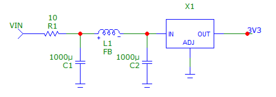
You can also cheat, by building a current divider, like so:
enter image description here

HF supply current for your micro will loop through local decoupling caps. Lower frequencies come from the LDO, which pulls that current from its input. I just used LM317 symbol for illustration.

The idea is to put a current divider at the input of the LDO with a pretty high resistor value and a large cap. You can also add ferrite beads to stop any HF noise from the micro leaking into your supply. When doing so, LDO input current will come from the lowest impedance source, which above 100Hz will be the capacitor. And the interesting thing is that your micro's ground currents will also return to the cap, not all the way to the power connector. So if you put the cap and the LDO somewhere in the upper left corner of your board, you can control the path your ground currents will take, and keep them away from the analog ground plane. You can even get fancy and use a second order RCRC filter, for example. Resistor value should be high, as you want voltage on the cap to ripple according to varying current drawn by the micro, so the current comes from the cap and not the power supply. If you want to be fancy, you could even replace it with a gyrator, to emulate a big inductor, but honestly a resistor is fine. This method works very well, but it needs a large cap, preferably with a low ESR. You've got low voltages though, so that won't be expensive.

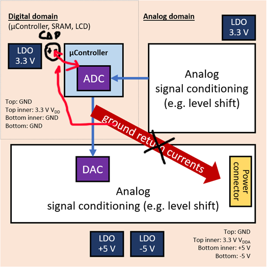
If you want to minimize ground plane pollution, you also have to place your caps the opposite of the usual way. It tends to be "intuitive" to put the cap on the power pin because "duh it's a power decoupling cap". But if you put the GND pin of the cap next to the GND pin of the load instead, current will go through a shorter path in your ground plane. The ideal is of course when the chip has a nice pinout with GND and VCC next to each other so you can squeeze in the cap right there. But for the large pre-LDO cap, think about putting its GND pin next to the micro's ground pins. Doesn't matter if the power route to the LDO is 1cm longer. Basically something like that:
enter image description here

In addition, this large cap keeps the micro's pulsed currents not just out of your ground, but also out of the power supply, so it stays clean, and your opamps will be happy.

Note the ADC performance isn't stellar:

enter image description here

I'm not sure about the jitter performance of the micro's timer either.

The layer stackup is also weird, if you're using 4 layer.

If you have components on top, then you can't have a ground plane on top, because it won't be a ground plane, it'll be full of holes and cuts. If you want the return currents from your I2S and other digital signals to travel in the ground plane in a civilized way right under the trace, then you must put an unbroken GND plane on layer2, which on 4 layer is right below toplayer and very close. Then you get good coupling between toplayer and layer1, which means low noise and low emissions.

Then you no longer have a 3V3 plane but that's not a problem, your DAC chips don't have that many power pins, so you can just route power locally. Decoupling caps are more effective when inductance to ground is lower, which you will get if ground is only 0.2mm below on layer2. And since your DACs will draw pulsed HF currents, a ferrite bead on DVCC also helps keeping the main power supply clean. Ferrite beads and caps also make current dividers, which keep HF ground currents local, so you can split your board into little isolated islands which don't pollute each other. Make sure the beads don't ring with the caps.

Or you can put a power island on layer3 or layer4, if you don't need -5V there.

Also if you run opamps on +/-5V, and that comes from a SMPS, remember opamps' PSRR sucks at high frequency, so a simple filter with a ferrite bead helps a lot. For the same reason it would be a bad idea to use an isolated switching DC-DC, or any kind of DC-DC in the vicinity, without extra care about filtering, because these make a lot of noise that is correlated with current, and that is correlated with signal, so you get signal dependent noise.

On the matter of opamps, if you use them in inverting mode, you can add a bunch of resistors and turn that into a substractor, which means a differential input. So it can sense ground at the source of the signal, not necessarily at the spot in the ground plane where the feedback resistor happens to be, and that has much better rejection. Basically, read this.

\$\endgroup\$
8
  • \$\begingroup\$ Many thanks for the write-up. Much appreciated.I still have to mull over some of what you've written. I know the internal ADCs aren't the best but I think they are good enough for my needs. Since it's for audio purposes, I can use oversampling. According to the datsheet, I can get an ENOB of up to 15.6 bits. I don't use SMPS anywhere. I use low-noise LDOs instead. Is it critical to have GND next to the top layer or can I keep 3.3 V right below the top and have GND below that? \$\endgroup\$
    – Hansel
    Commented Dec 28, 2021 at 16:20
  • \$\begingroup\$ My 3.3 V supply is already placed next to the µController, and so are the decoupling caps. The local decoupling caps are placed right underneath the balls on the opposite side of the PCB. The DAC is controlled via an SPI interface (up to 50 MHz). \$\endgroup\$
    – Hansel
    Commented Dec 28, 2021 at 16:20
  • \$\begingroup\$ If you put 3V3 on layer2, then signal traces on top layer will couple with it instead of coupling with ground plane below. When they leave the 3V3 plane, there will be a discontinuity, and return current will find a way through the closest 3V3 decoupling cap into the ground plane. Also in places where you don't have the power plane, ground plane will be much further away (1.4mm instead of 0.2mm) so much less effective, like a 2 layer board instead of 4 layer. \$\endgroup\$
    – bobflux
    Commented Dec 28, 2021 at 17:29
  • \$\begingroup\$ OK, thanks. I understand. \$\endgroup\$
    – Hansel
    Commented Dec 28, 2021 at 18:19
  • \$\begingroup\$ I've looked at your post further. Luckily, I am already using power islands. The LDOs I mentioned have very good PSRR, so I think I don't need to worry about the kickback of the LDOs into the supply. The µC is already coupled via ferrite beads. \$\endgroup\$
    – Hansel
    Commented Dec 28, 2021 at 18:24
2
\$\begingroup\$

If you can, I would suggest using a multi-layer PCB with multiple GND panes, e.g.:

  1. signals (and probably some VCCs), components + rest filled with GND
  2. DGND
  3. AGND (where needed) and VCCs (in the digital domain)
  4. signals (and probably some VCCs), components + rest filled with GND

or even better using 6 layers:

  1. signals (and probably some VCCs), components + rest filled with DGND
  2. VCCs
  3. DGND
  4. AGND
  5. DGND (or VCCs)
  6. signals (and probably some VCCs), components + rest filled with DGND

Only connect AGND and DGND in one point (using one or multiple vias next to each other). Probably best close to the controller, i.e. where ADC/DAC and the digital domain meet each other.

If you can't use separate DGND/AGND layers, probably you'll get the best result using one common GND layer with as much as possible filled with copper (i.e. everything except the vias).

As proposed in the other reply, using LC-filters* in front of the analog VCC supply domain or in front of every analog device group (i.e. 1x for ADC+Vref and 1x for DAC+Vref) improves the decoupling, so the noise generated by the digital domain and the microcontrollers won't negatively influence the analog circuit. (*small L in the order of 1-10 uH and C in the order of 1-100 µF - you may want to simulate inrush currents and use an 1-4.7 R resistor to limit it if the voltage drop doesn't matter much)

\$\endgroup\$
1
\$\begingroup\$

GND signals of digital electronic integrated circuits should be connected to "ground planes" of the boards. They are solid copper planes.

Ground planes of the board shoud be connected to the the board's connector GND pin.

Examples of digital electronic integrated circuits

  1. Microcontrollers

  2. Led or relay drivers

  3. RS232 or RS485 interface circuits

  4. RAM and Flash memories


ADC's, DAC's, and Operational Amplifiers ground signals should be connected to voltage regulator GND pin using a single wide PCB trace.

That trace should not cut any ground plane.

Route that trace on a signal layer using vias.

\$\endgroup\$
1
  • \$\begingroup\$ Would you care to explain why this should be the correct way of doing it? If it's done as described by you, it seems to go counter to the idea to keep the current return paths along the trace the signal came from as the return current is forced it to take the longer route towards the star-connected LDOs. \$\endgroup\$
    – Hansel
    Commented Dec 28, 2021 at 10:46

Your Answer

By clicking “Post Your Answer”, you agree to our terms of service and acknowledge you have read our privacy policy.

Not the answer you're looking for? Browse other questions tagged or ask your own question.