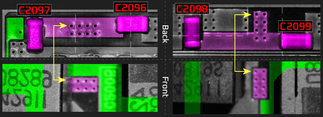
NOTE: It turns out, the ground connections I wonder about below actually are connected (thanks Sim Son in comments), although I still cannot see how they could be connected (additional closeups). The reason I initially concluded they weren't connected was a combination of being unable to see connections on the PCB (still can't) along with, as it turns out, a broken probe on the meter I was using for continuity checks. So the main premise of this question appears to be incorrect; although the questions about the effect of said ground still stand.
I am looking at the audio amplifier section from a mainboard scavanged from an LCD TV (Sony BU Board, P/N 1-876-561-13, TV appears to be a KDL-40V4150). The amp circuit is built around a TI TPA3100D2PHPR chip (20W stereo class-D amp). The PCB appears to be a 2-layer board.†
I have been studying it, as I made a project out of cutting this section out of the mainboard and using it as a standalone amp (mostly worked). However, while closely examining it I noticed what appears to be an unexpectedly absent ground connection in the output section, and I'm not sure what to make of it.
Schematics
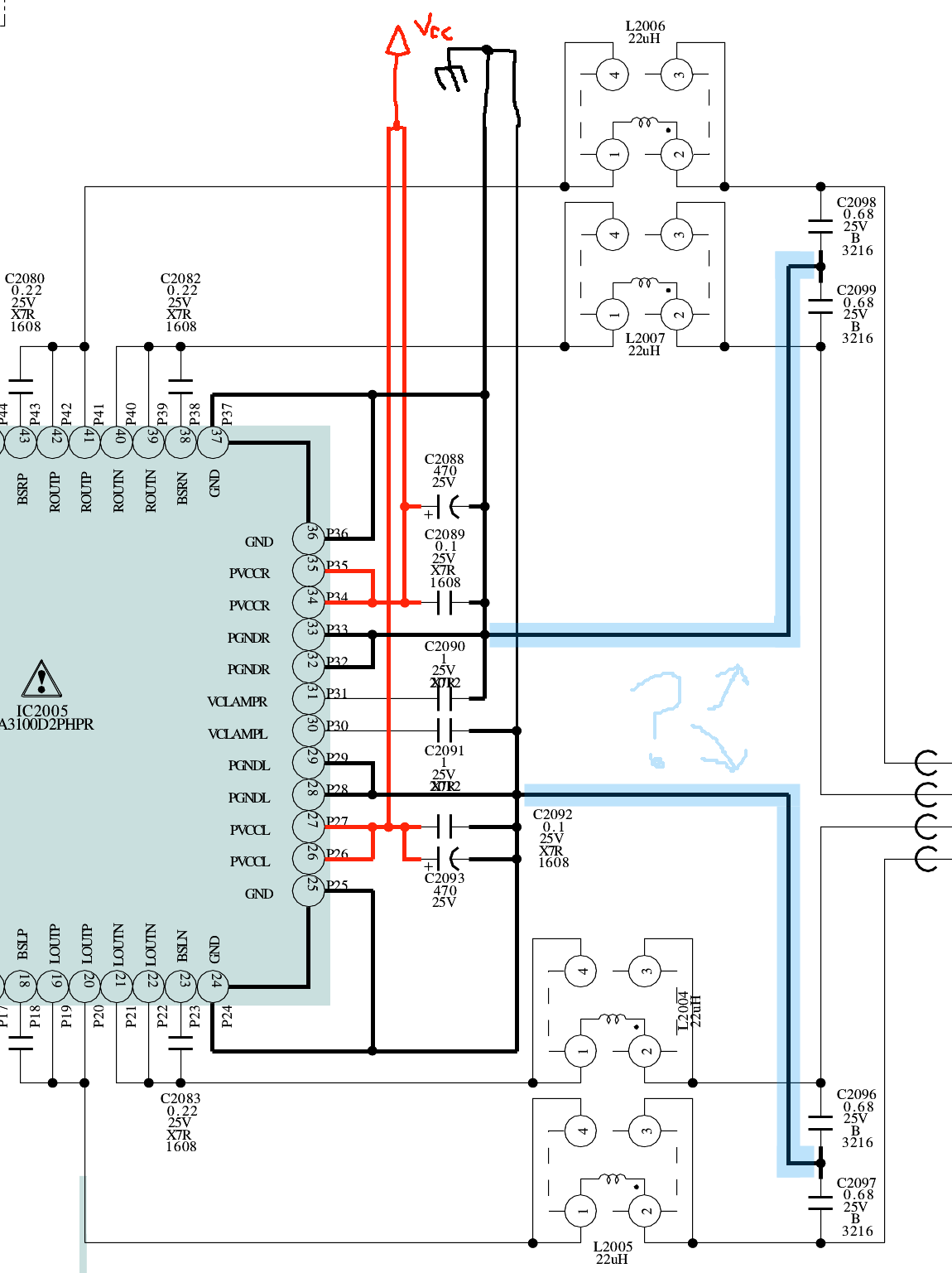
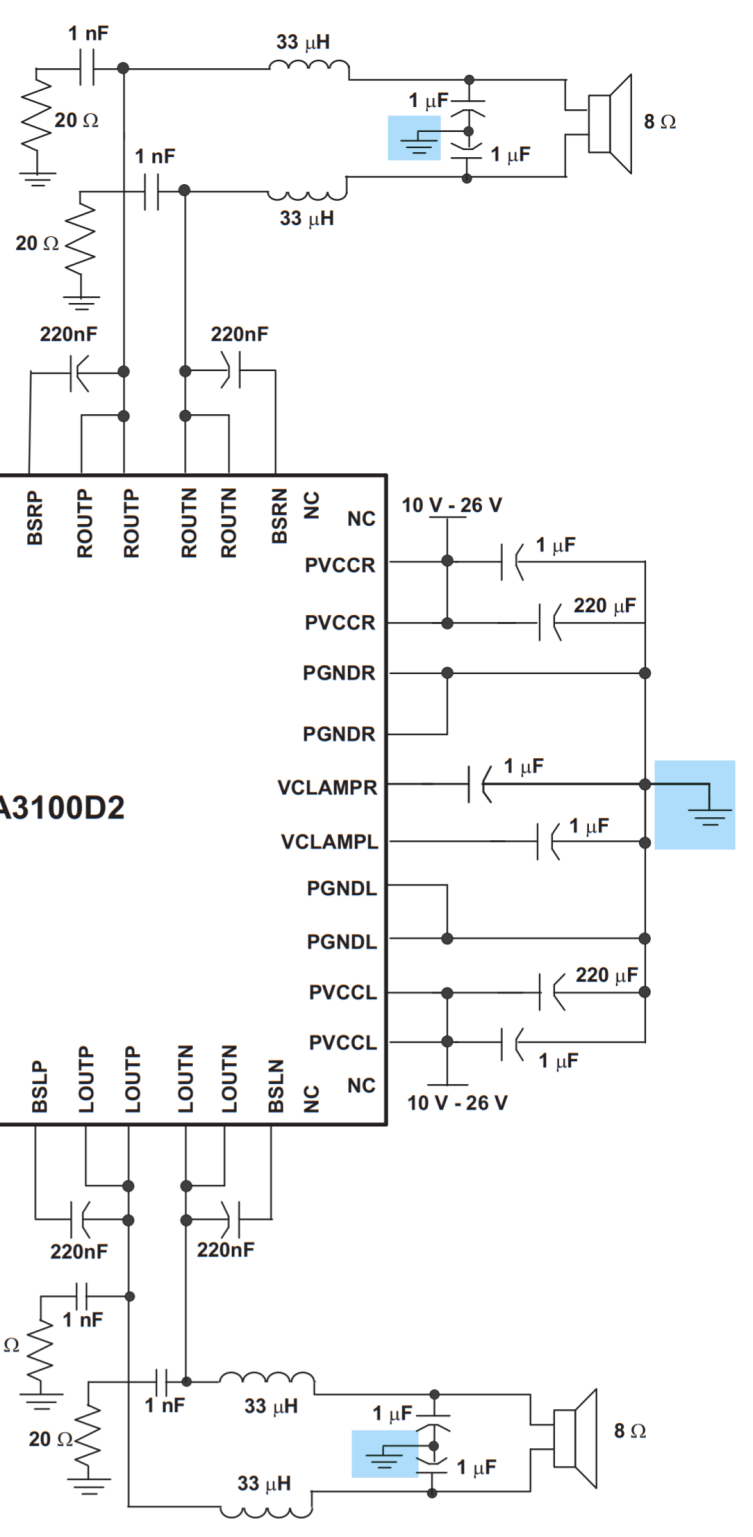
Here is part of the schematic from the TV's service manual and the corresponding part of the example circuit in the chip's datasheet (click for high res). The only difference that might be relevant (?) is the Sony circuit doesn't have the 1nF + 20Ω decoupling bits off the outputs before the inductors. I've highlighted the suspicious ground connections in blue:
Notes:
- Sony uses this board (or slight variants of it) in a bunch of TVs. I'm confident this is the correct service manual as I found the model # of the TV printed on the chassis.
- I assume that Sony uses this amp circuit in other products as well, since it is relatively self contained and I see lots of unused pads that I assume are for parts in other variants.
PCB
That's all fine, but the reason for my question is the PCB appears to not include the ground connections highlighted above.
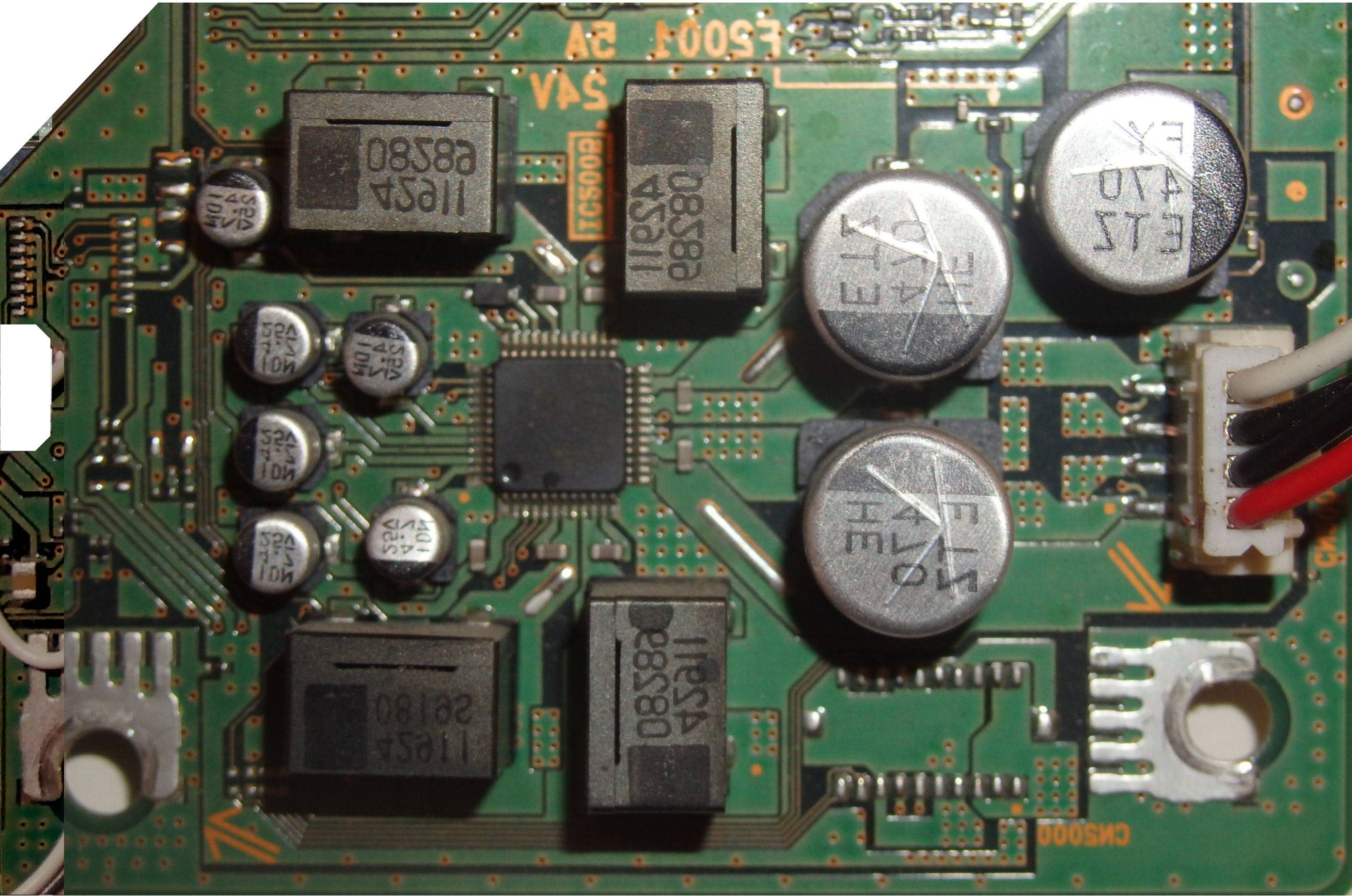
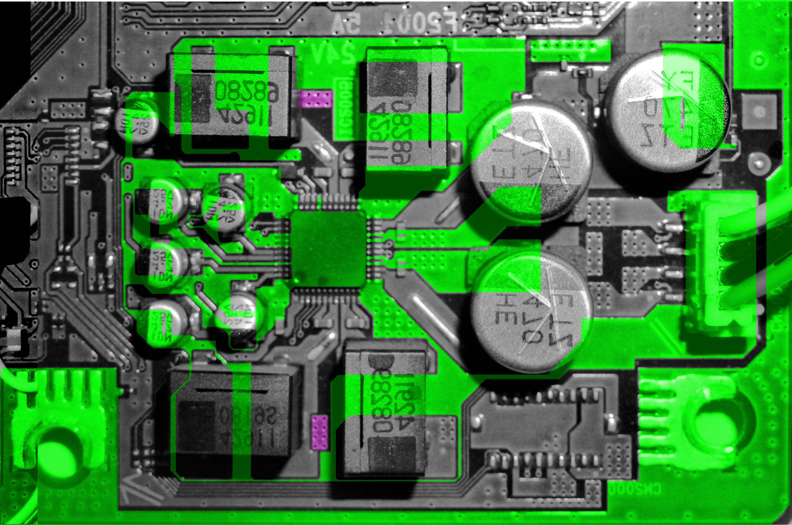
I manually followed all the ground traces on the PCB. Descriptions are with the images below (click to enlarge), the general components of interest are the capacitors after each inductor (C2096 thru C2099):
| Description | Back | Front |
|---|---|---|
| TI chip in center. | 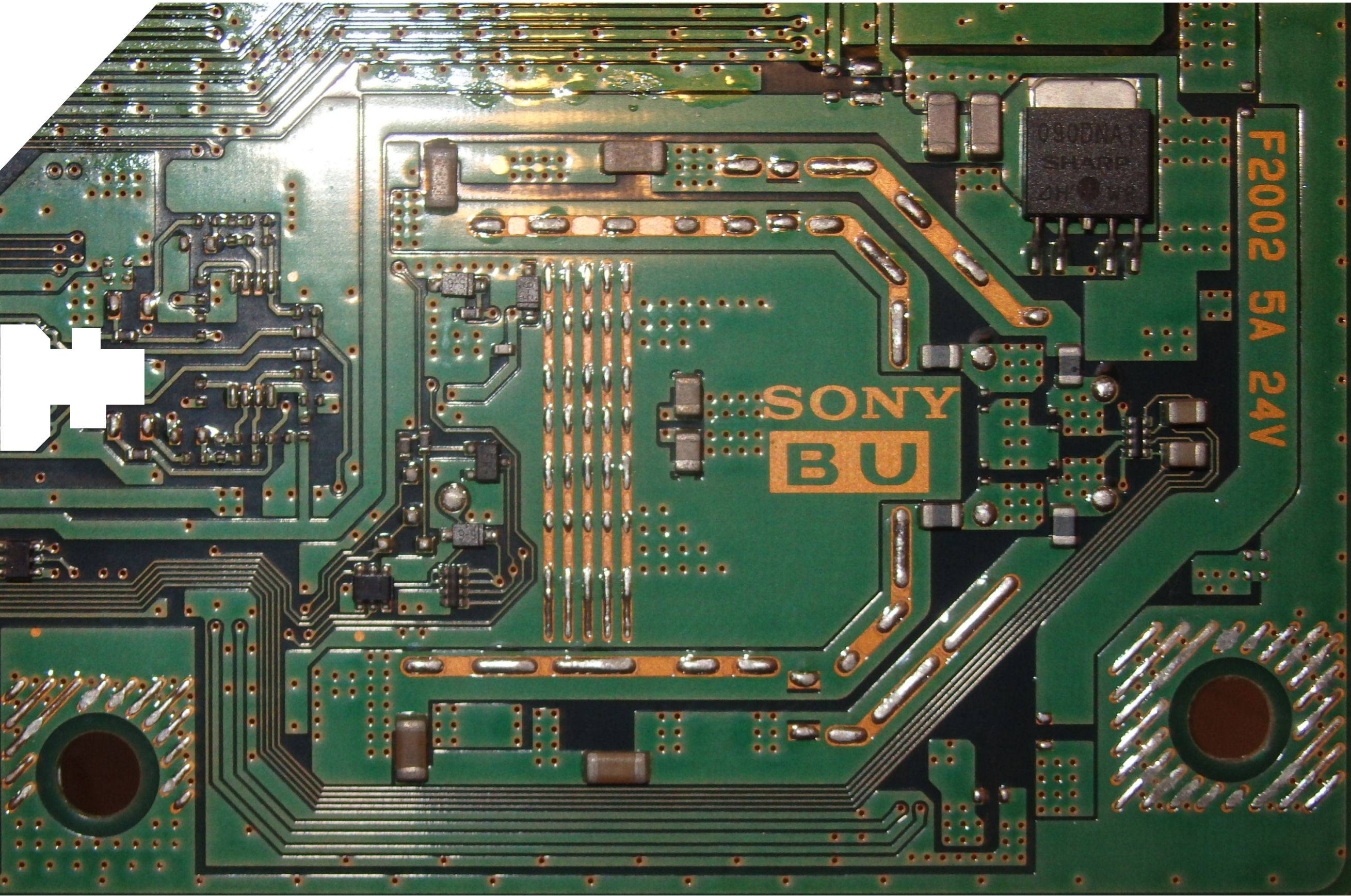 |
 |
| Ground trace is green. Caps and the traces between them are purple. | 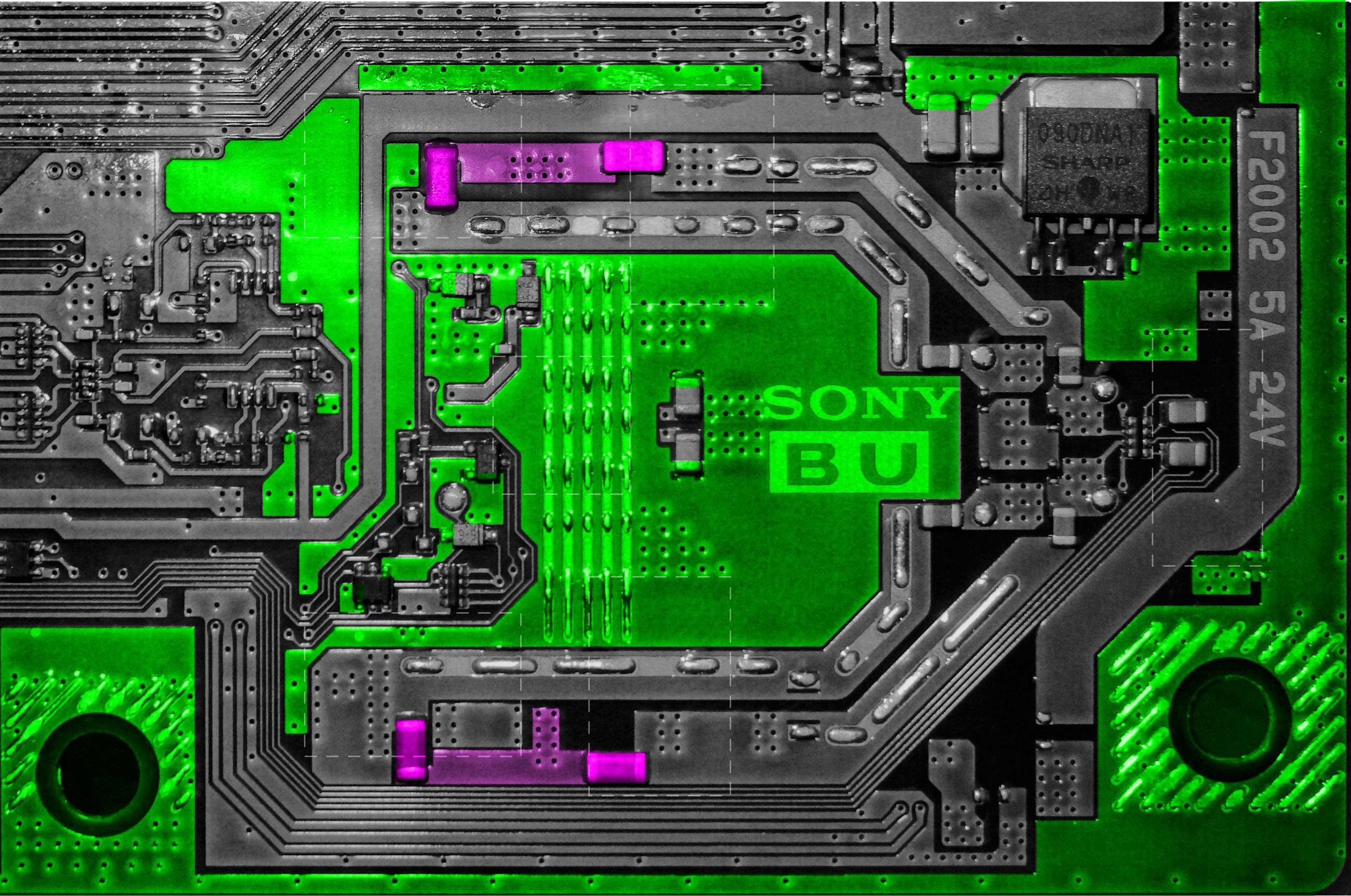 |
 |
| Back image also shows front traces. Front image is service diagram instead of photo. | 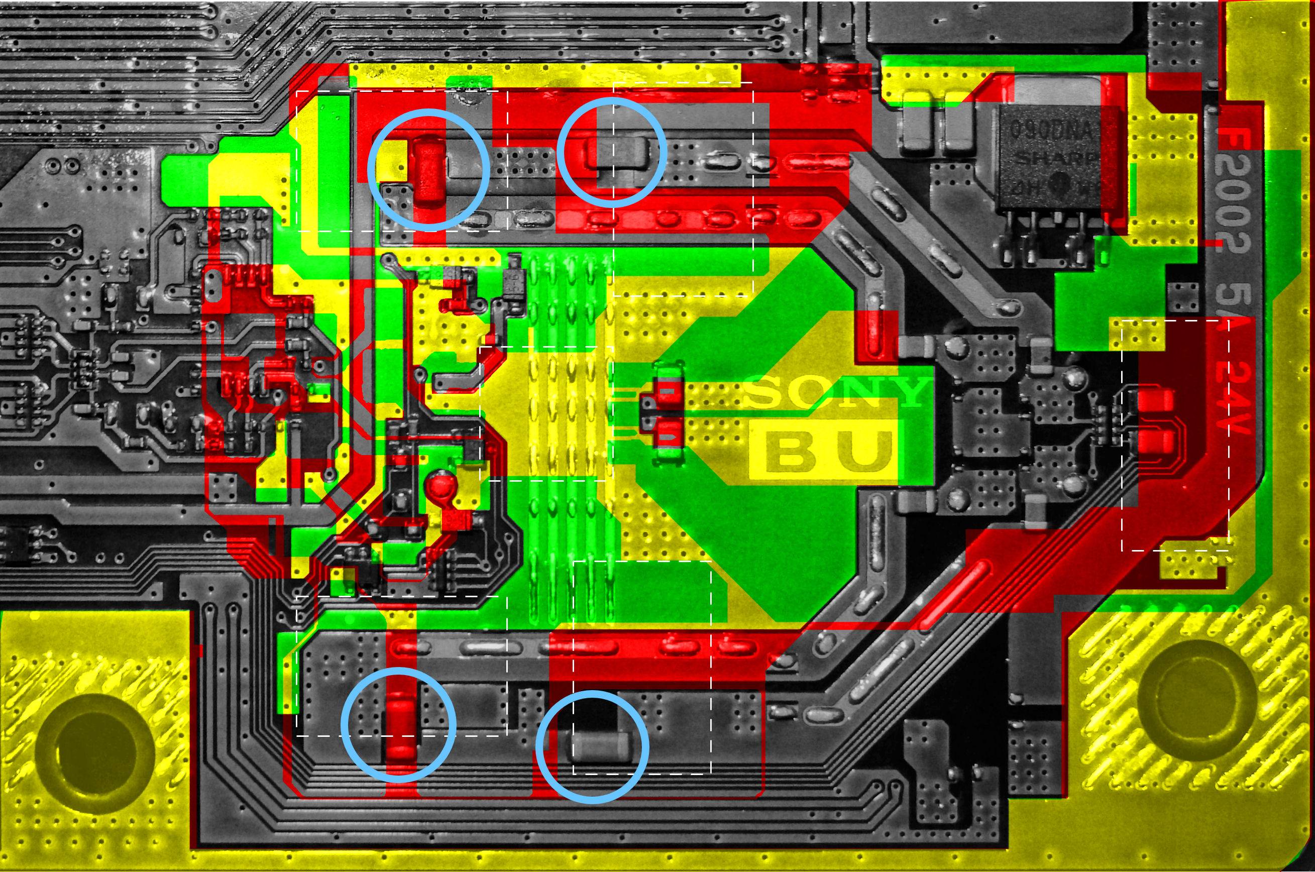 |
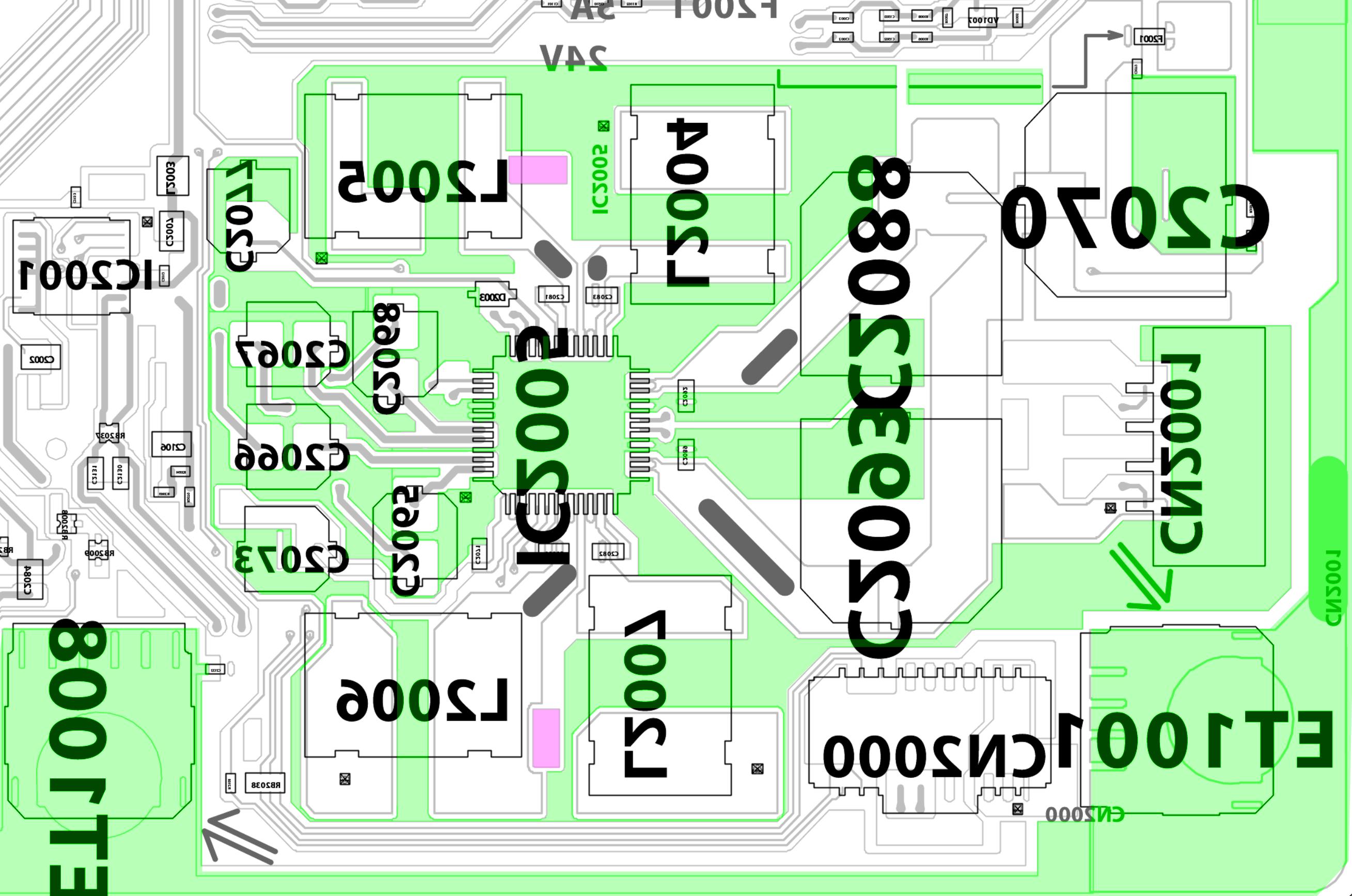 |
The confusing bit is here:
The grounds are green and the caps and traces between them are purple. Unless I'm missing something, there is no connection on the PCB between the purple and the green. This would mean that the connections that I highlighted in the schematics aren't present.
Question
So that was a lot of pictures but my question is:
Why might those connections be missing? Is it some other common configuration for a class-D amp's output that I don't know about? Is it related to the lack of decoupling capacitors at the chip's outputs before the coils?
Also, how does that ground affect the amp's behavior?
Basically: What's going on here?
Note: The outputs of this circuit go to two places: directly to the TV's internal speakers, and also to some other amp that drives the line-out jacks. There's some resistors and capacitors there too, not sure if they're relevant, but here is that part of the circuit.
† There is strong evidence that the PCB is only 2 layers:
- I cut this from the main board with a bandsaw and only saw two layers on that border.
- I am able to account for every connection on the schematic with the visible PCB traces except for this ground (I checked carefully, every component, in the amp section as well as the main audio processor and aux amp).
- The service manual's PCB layouts (page 54) show two layers only, and have no indications of blind vias or traces.
- It would be trivial to route those to the ground trace. The purple and green areas (from my images) are directly adjacent on the front side of the board.
So under the assumption that cost reduction is important, it seems to me like it would be strange for the PCB to have another layer just for a few connections that could just as easily be made on the existing layers.

