1
\$\begingroup\$

I'm trying to understand a Wien Bridge oscillator circuit as published in Elektor 7/1987 on page 63, and I'm getting kind of frustrated. I've reviewed plenty of theory in an attempt to revive my BEng EE knowledge, incl. consuming mind-numbing amounts of Art of Electronics, but still seem to fail at understanding trivial circuits.

As a bit of a preface, I understand Wien oscillator operation in general - why the gain has to be exactly 3 to maintain oscillation, how the RC stages work, JFET AGC with linearisation, or in this case diodes, lamp compensation etc. etc. I also thought I understood the basic workings of op-amps but perhaps not.

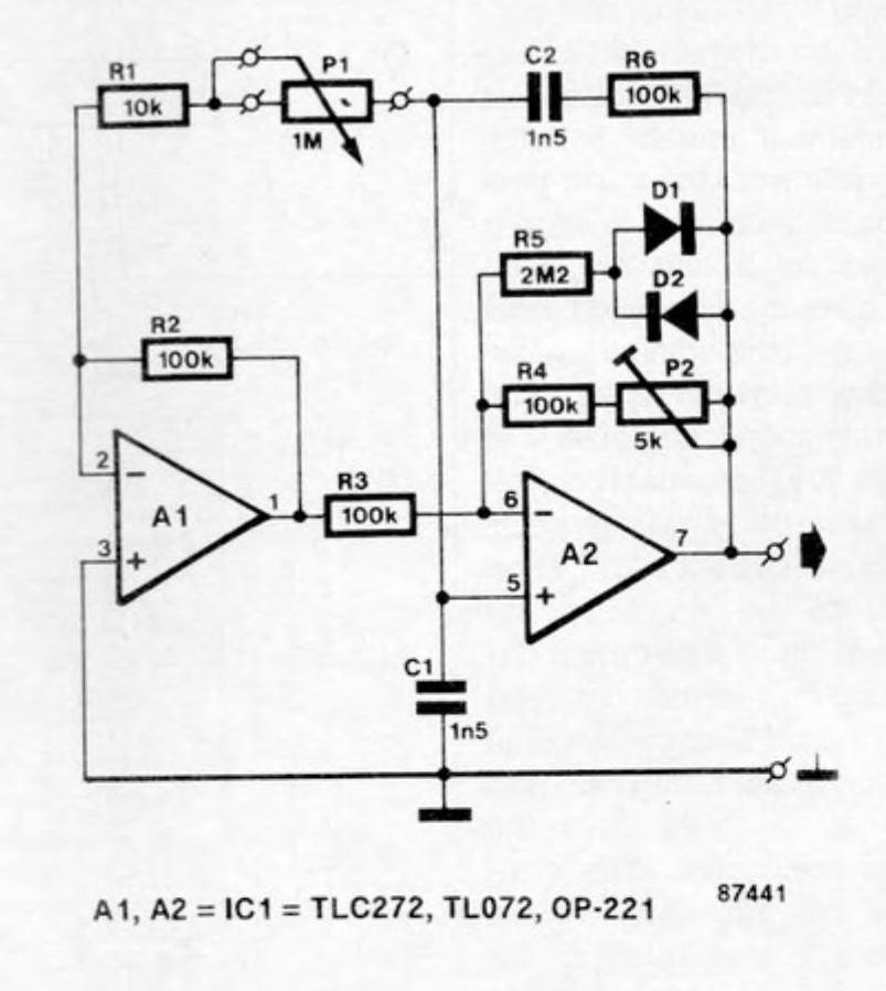
Here is the circuit I am talking about, taken from the resource mentioned above:

enter image description here

The magazine claims that this is frequency variable using potentiometer P1. I have seen dual op-amp oscillators happily interfere with just one RC pair to change frequency, so I don't doubt this claim. Though this does bring up side question one:

Side Q1: Does the asymmetric RC adjustment (i.e. leaving C2 and R6, while playing with the C1, R1+P1 pair) cause significant distortion? If so, what is the nature of this distortion? Why does doing this with a single op-amp oscillator almost certainly cause the oscillator to fail?

I can understand most of what's going on in this circuit, especially what's going on on the right half. It's the action of A1 that I am most confused about. (Note that I have tried and failed to simulate this circuit in Falstad and LTSpice.)

It appears to me like an inverting op-amp with loop gain determined by -R2/(R1+P1), buffered by R3 into the inverting input of A2. Here come the questions:

Q1: What is the effect of having A1's output driving A2's - input? In a classic design with a single op-amp, R3 would lead into ground. Is A1's output somehow appearing equivalent to ground using some "virtual ground" trickery? What is the significance of this? What effect does this have on the circuit? Most importantly, why is this being done?

Q2: How does having A1 driving "node 6" not have an impact on the behaviour of the oscillator as a whole. Sure, A2 has hi-Z inputs, but what's stopping current running into and out-of the network containing R5, R4 et. al. Is this okay because A1 can source and sink current just as having "node 1" be ground would?

I'm sure I have a couple of major misunderstandings strewn in here for good measure.

EDIT:

I have modified Neil's circuit from below into a more traditional design to illustrate the nature of this question:

Neil's circuit modified

Note that this is fixed frequency, and omits A1. Modifying R1 in this case causes SPICE to have a fit and get caught up about 200ms into the transient simulation. It also seems to ramp to oscillation rather slowly. Why is A1 needed to enable variable frequency?

\$\endgroup\$
2
  • \$\begingroup\$ Get hold of a free and freely available simulator and take a voyage of discovery on this. \$\endgroup\$
    – Andy aka
    Commented Dec 31, 2021 at 9:19
  • \$\begingroup\$ Do you know what condition the circuit needs to meet to oscillate in the first place? Play with this tinyurl.com/yxuo953v \$\endgroup\$
    – G36
    Commented Dec 31, 2021 at 11:58

2 Answers 2

2
\$\begingroup\$

This is not a Wien bridge oscillator, though it's trying a bit to look like one.

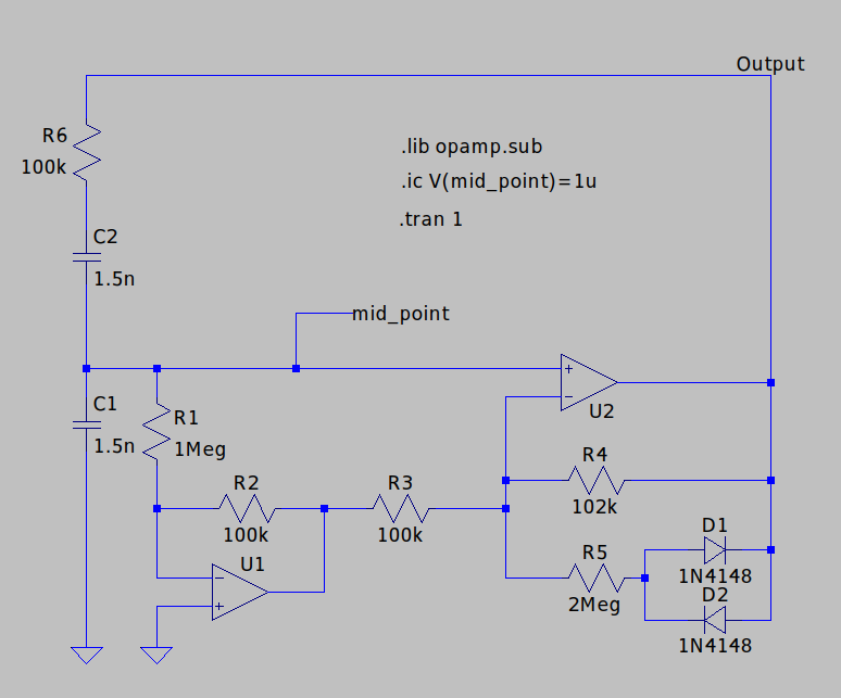
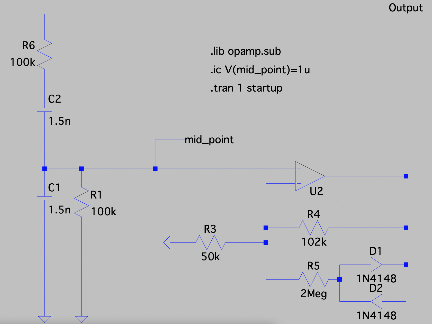
I've redrawn it slightly, to emphasise the 'Wien' components R6, C2 in series and C1 and R1 in parallel to ground. This schematic is drawn with LTSpice. The reference designators are the same as those in the question.

enter image description here

U1 with R2 is a virtual ground amplifier, presenting a short circuit to the bottom of R1. It's a transconductance amplifier with a gain of R2, producing a voltage at its output of 100k x -I(R1). It's basically measuring the current in R1.

The R4/5/D1/2 network around U2 is intended to produce an effective feedback resistance of 100k at the correct output level. At a lower level, D1/2 stop conducting and the feedback resistance rises, and vice versa. This creates a feedback network together with R3.

U2 is a differential amplifier, with inputs from both V(mid_point), and U1. It can be analysed by fixing one input, computing the gain for the other, and then superposing the two results.

With U1 output fixed, the output of U2 is 2 x V(mid_point).

With V(mid_point) fixed, the output of U2 is -1 x U1 output, or 100k * I(R1).

It seems to me that the V(midpoint) and I(R1) will always be in phase. It appears that it's the phase shift through R6 and C2 into the C1/R1 load that controls the resonant frequency.

That's as far as I'm going to go with a verbal description. It needs somebody to do nodal analysis and write down the phase shifts and amplitudes to demonstrate that there is a resonant frequency where the gain round the loop is unity with zero phase shift.

Simulating the circuit in LTSpice, I get the following approximate frequencies

R1(Ω) freq(Hz)
1k 10k
10k 3k
100k 1k
1M 300

So it's not behaving like a Wien Bridge oscillator with a linear dependence on tuning resistance, it's going as the square root of R. The circuit appears to be behaving as if it's synthesising an LC, with the value of one of them linearly related to the tuning resistance. It's an interesting circuit though. As R1 needs to swing over such a wide range, it's of limited usefulness. I'd be inclined to use a state variable oscillator if I needed a wide range oscillator and could afford multiple opamps.

The vital part that some people miss when trying to simulate an oscillator in Spice is the .ic Initial Conditions. When Spice first analyses a circuit, it does a DC analysis to find the operating voltage of all the capacitors. Now settled, the circuit has no stimulus to start oscillating, unlike a real oscillator which starts from noise. Setting an initial voltage on one of the capacitors forces an initial transient into the circuit.

I've included my LTSpice .asc file below for your simulating convenience.

Version 4
SHEET 1 912 836
WIRE 720 -224 -64 -224
WIRE -64 -176 -64 -224
WIRE -64 -48 -64 -96
WIRE 240 48 176 48
WIRE -64 112 -64 16
WIRE 16 112 -64 112
WIRE 176 112 176 48
WIRE 176 112 16 112
WIRE 480 112 176 112
WIRE 720 128 720 -224
WIRE 720 128 544 128
WIRE -64 144 -64 112
WIRE 16 144 16 112
WIRE 480 144 416 144
WIRE 416 240 416 144
WIRE 480 240 416 240
WIRE 720 240 720 128
WIRE 720 240 560 240
WIRE 16 272 16 224
WIRE 80 272 16 272
WIRE 208 272 160 272
WIRE 256 272 208 272
WIRE 416 272 416 240
WIRE 416 272 336 272
WIRE 624 320 576 320
WIRE 720 320 720 240
WIRE 720 320 688 320
WIRE 16 352 16 272
WIRE 80 352 16 352
WIRE 416 352 416 272
WIRE 480 352 416 352
WIRE 576 352 576 320
WIRE 576 352 560 352
WIRE 208 368 208 272
WIRE 208 368 144 368
WIRE 80 384 16 384
WIRE 576 400 576 352
WIRE 624 400 576 400
WIRE 720 400 720 320
WIRE 720 400 688 400
WIRE -64 432 -64 208
WIRE 16 432 16 384
FLAG -64 432 0
FLAG 16 432 0
FLAG 720 -224 Output
FLAG 240 48 mid_point
SYMBOL OpAmps\\opamp 112 304 R0
SYMATTR InstName U1
SYMBOL OpAmps\\opamp 512 192 M180
SYMATTR InstName U2
SYMBOL cap -80 144 R0
SYMATTR InstName C1
SYMATTR Value 1.5n
SYMBOL cap -80 -48 R0
SYMATTR InstName C2
SYMATTR Value 1.5n
SYMBOL res 0 128 R0
SYMATTR InstName R1
SYMATTR Value 1Meg
SYMBOL res 176 256 R90
WINDOW 0 0 56 VBottom 2
WINDOW 3 32 56 VTop 2
SYMATTR InstName R2
SYMATTR Value 100k
SYMBOL res 352 256 R90
WINDOW 0 0 56 VBottom 2
WINDOW 3 32 56 VTop 2
SYMATTR InstName R3
SYMATTR Value 100k
SYMBOL res 576 224 R90
WINDOW 0 0 56 VBottom 2
WINDOW 3 32 56 VTop 2
SYMATTR InstName R4
SYMATTR Value 102k
SYMBOL res 576 336 R90
WINDOW 0 0 56 VBottom 2
WINDOW 3 32 56 VTop 2
SYMATTR InstName R5
SYMATTR Value 2Meg
SYMBOL res -48 -80 R180
WINDOW 0 36 76 Left 2
WINDOW 3 36 40 Left 2
SYMATTR InstName R6
SYMATTR Value 100k
SYMBOL diode 624 336 R270
WINDOW 0 32 32 VTop 2
WINDOW 3 0 32 VBottom 2
SYMATTR InstName D1
SYMATTR Value 1N4148
SYMBOL diode 688 384 R90
WINDOW 0 0 32 VBottom 2
WINDOW 3 32 32 VTop 2
SYMATTR InstName D2
SYMATTR Value 1N4148
TEXT 296 -144 Left 2 !.lib opamp.sub
TEXT 296 -104 Left 2 !.ic V(mid_point)=1u
TEXT 294 -60 Left 2 !.tran 1
\$\endgroup\$
5
  • \$\begingroup\$ But this is a Wein bridge (R6+C2 and R1||C1). R1 is a part of a Wien bridge too. Notice that for R1 = R6 the A2 , A1 gains together is (1 + R4/R3) + R4/R3*R2/R1 = 3 V/V . And this is exactly what we need in Wein Bridge when R6 = R1; C1 = C2. But when we change the R1 we also change the bridge gain, But at the same time, A1 will compensate for this (increases the loop gain) \$\endgroup\$
    – G36
    Commented Dec 31, 2021 at 12:31
  • \$\begingroup\$ Thanks for the analysis. I would say I expect a sqrt dependence in a Wien Bridge (f=1/2\pi\sqrt{R_1R_2C_1C_2}). Could you explain the charging impedance for C1? How does R1 see ground through the op amp? \$\endgroup\$ Commented Dec 31, 2021 at 13:45
  • \$\begingroup\$ R1 is connected to U1's -ve input. U1's +ve input is grounded. U1 has feedback, and is active. Therefore U1 forces its -ve input to be the same voltage as its +ve input, ie 0 V. This configuration is also known as a 'virtual ground'. What's a 'charging impedance'? C1 is driven from the output by C2 and R6, and loaded by R1 to (virtual) ground. You can calculate the impedance of those components if you feel like it. \$\endgroup\$
    – Neil_UK
    Commented Dec 31, 2021 at 14:00
  • \$\begingroup\$ The output frequency is \$ \large Fo = \frac{1}{2 \pi R_6 C_2} * \sqrt{a}\$ where a = R6/R1. but still it is Wien bridge oscillator. \$\endgroup\$
    – G36
    Commented Dec 31, 2021 at 14:50
  • \$\begingroup\$ I have added an edit to my question with a more traditional version of your LTSpice circuit. Could you shed light on the utility of A1? Is it needed to enable variable frequency? Thanks. \$\endgroup\$ Commented Dec 31, 2021 at 17:08
1
\$\begingroup\$

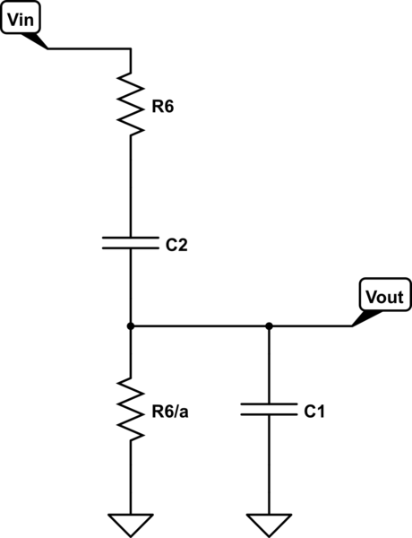
In this circuit, The " Wien Bridge" is (R6, C2) series network and the parallel part is C1 (R1+P1).

In a traditional bridge circuit, we have R6 = R1 and C1 = C2, and the bridge attenuation is 1/3. So, if you want to change the frequency of an oscillation in a "traditional circuit" you need to change R6 and R1 (R1 + P1) if you want to keep the "gain stage" unchanged (Av = 3).

But in your circuit, we have a different situation:

schematic

simulate this circuit – Schematic created using CircuitLab

This time the attenuation factor at \$ \large Fo = \frac{1}{2 \pi R_6 C_2} * \sqrt{a}\$ is no longer constant and equal to 3.

The new attenuation factor is equal to :

\$ \Large \frac{1}{2 + \textrm{a}}\$ (For C1 = C2 and R1 = R6/a).

So we need to compensate for this loss to meet the oscillation condition ( Barkhausen criterion).

And this is the job for A1 and A2.

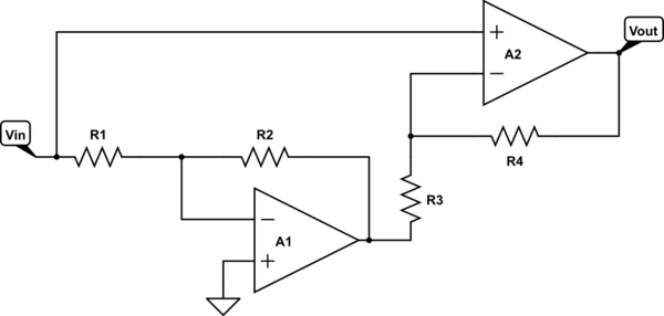
schematic

simulate this circuit

The voltage gain of this amplifier is:

\$\Large A_V = (1 + \frac{R_4}{R_3}) + \frac{R_4}{R_3} \frac{R_2}{R_1}\$.

And if R4 = R3 = R2 = R6 the amplitude condition will be met when:

\$ \left((1 + \frac{R_4}{R_3}) + \frac{R_4}{R_3} \frac{R_2}{R_1}\right)\frac{1}{2 + \textrm{a}} =1\$

\$\Large R_1 = \frac{R_6}{a}\$

And this is what we have in this circuit. R1 is the part of a gain stage and the Wien bridge at the same time. It is possible thanks to the "virtual ground" provided by A1 and its negative feedback. Thanks to this we can now change the frequency of an oscillation using only a single variable resistor.

\$\endgroup\$
5
  • \$\begingroup\$ "R1 is the part of a gain stage and the Wien bridge at the same time. It is possible thanks to the "virtual ground" provided by A1 and its negative feedback." But why is this needed over a more traditional design? I imagine it's needed to allow for variable frequency with R1, but I don't understand the necessity. \$\endgroup\$ Commented Dec 31, 2021 at 16:56
  • \$\begingroup\$ R1 is not special. It simply sets the minimum resistance of the potentiometer P1. Alone, P1’s minimum resistance is 0, but the circuit is not functioning well then. So R1 sets a minimum so that the frequency won’t go beyond what the circuit was designed to do. \$\endgroup\$ Commented Dec 31, 2021 at 17:36
  • \$\begingroup\$ To simplify the equation I use R1 instead of R1 = (R1 + P1). \$\endgroup\$
    – G36
    Commented Dec 31, 2021 at 18:14
  • \$\begingroup\$ If you want to change the frequency of an oscillation in a "traditional circuit" you need to change R6 and R1 if you want to keep the "gain stage" unchanged (Av = 3). But if you change the R1 resistor value, you need to modify the gain as well. For example, if you use R1 = 50k. So, you need to change the gain for 3 to 1/(2 + 2) = 4. But we can overcome this by adding A1 stage. And using R1 as a gain setting resistor as well. \$\endgroup\$
    – G36
    Commented Dec 31, 2021 at 18:16
  • \$\begingroup\$ Ah, I'm kind of frustrated I overlooked that! Too many late nights staring at this I think. Thanks for clearing that up! It all makes sense now! \$\endgroup\$ Commented Jan 1, 2022 at 1:05

Your Answer

By clicking “Post Your Answer”, you agree to our terms of service and acknowledge you have read our privacy policy.

Not the answer you're looking for? Browse other questions tagged or ask your own question.