1
\$\begingroup\$

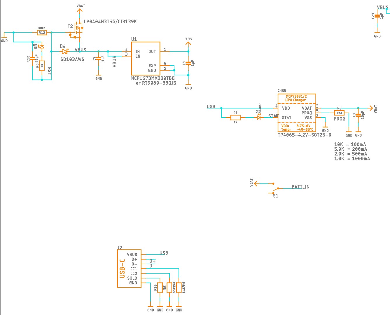
I am making a custom PCB for an ESP32-S2 chip and the LDO controller is returning me 1.88 V instead of 3 V. Of course this is not enough for the ESP, but no matter what I do I can't get it to work.

At first it was returning something around 1.15 V, I guessed it was a bad solder connection, so I warmed up the regulator and MOSFET and now I get that 1.88 V on USB, and even less over the battery.

The LDO is more or less taken from TinyPico and theoretically should work, so I wonder what I could have done wrong.

I measured with a multimeter a few places around the regulator and for some reason the MOSFET appears about 1.2 V less than the USB and the regulator reduces that from about 3.8 V to 1.88 V.

Regulator: ncp170amx300

MOSFET: lp0404n3t5g

Diode: bat60jfilm

enter image description here

\$\endgroup\$
3
  • 4
    \$\begingroup\$ The regulator you are stating is a different one than written in the schematic, could you verify that the pins on the footprint are the same one as given in the datasheet? \$\endgroup\$
    – Ananas_hoi
    Commented Feb 25, 2022 at 8:29
  • 1
    \$\begingroup\$ What’s the input voltage? How much current are you trying to source? \$\endgroup\$
    – winny
    Commented Feb 25, 2022 at 8:31
  • 1
    \$\begingroup\$ I think your FET has source and drain reversed. Is that body diode not going to have Vbat permanently connected? (Not saying this is necessarily going to be the cause of your 3V3 issue.) \$\endgroup\$
    – DiBosco
    Commented Feb 25, 2022 at 8:58

1 Answer 1

2
\$\begingroup\$

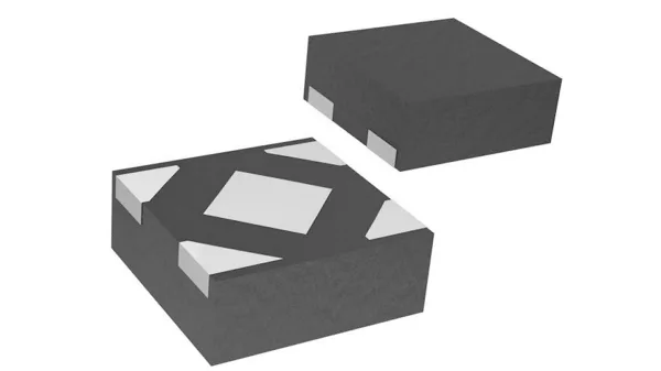
I will allow myself to make an assumption that you're NOT using ncp170amx300 XDFN4 package, because it's a BGA-like thing with pads all on the bottom.

XDFN-4:

enter image description here

Simply because it's a nightmare to work with when prototyping, and one requires hot air station. Totally unreasonable for amateur-level project.

Therefore, I will dare say you have a wrong pinout of the regulator. Pin 1 is OUT only on these XDFNs.

enter image description here

And yes, when you talk about chips in multiple packages, it's helpful to give the exact package you're using, since we're talking schematics. Because if you ARE using XDFN for a prototype (WHY?) then my answer is entirely irrelevant.

If you ARE, check IC orientation.

\$\endgroup\$
5
  • \$\begingroup\$ That is a nasty package, speaking as someone who does almost exclusively prototyping. \$\endgroup\$
    – Hearth
    Commented Feb 25, 2022 at 16:48
  • \$\begingroup\$ What's so nasty about it? 4 large pins and a center pad seem right down simple for a qfn. Dead bugging would be easy. What am I missing @Hearth? \$\endgroup\$
    – Passerby
    Commented Feb 25, 2022 at 16:54
  • \$\begingroup\$ @Passerby I suppose dead-bugging it would be simple enough. I was thinking about trying to solder it in the intended orientation, which makes anything with an exposed pad pretty awful. There is also the matter of its size, though--someone more skilled than I could maybe hand-solder wires to that without bridging, but I certainly couldn't. \$\endgroup\$
    – Hearth
    Commented Feb 25, 2022 at 16:55
  • \$\begingroup\$ Where are the high frequency bypass capacitors? \$\endgroup\$
    – Gil
    Commented Feb 25, 2022 at 20:24
  • \$\begingroup\$ SMT, even with weird pads, is actually easier to use with homemade PCBs because you don't need to drill anything to use them. You can make a breadboard adapter for that mount from single-side copper clad with a knife, no printing or etching needed... \$\endgroup\$
    – dandavis
    Commented Feb 25, 2022 at 22:31

Your Answer

By clicking “Post Your Answer”, you agree to our terms of service and acknowledge you have read our privacy policy.

Not the answer you're looking for? Browse other questions tagged or ask your own question.