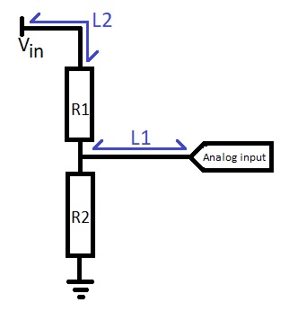
The question is simple, but the answer is all about details, and their ramifications.
The best placement of the voltage divider relative to the input connector and the ADC depend not only on the signal, but on the rest of the board design and possibly on the signal source and the nature of the cable from it to your board input connector.
I was going to ask you for all these details, but instead I think I'll go over some of the common ones that I know will make a difference, so you have an idea of how to determine the placement of the parts yourself. This is not an exhaustive list -- I'm leaving out thermal effects, the possibility of microphonics, anything I can't think of right now, etc. But I think these four points are a roundup of the most common things you need to think about.
- If the signal is slowly varying, and if the board itself and the environment it's in are electrically quiet (i.e. there's no high voltages or currents), then it doesn't matter.
- If the signal has high-frequency components, either because it's RF or because it has events (i.e. pulses) with sharp edges, then the cable from the source to the board is a transmission line that you want to match with your divider to prevent reflections on that cable, and if distance from your connector to your ADC is greater than about \$\frac{1}{10}^{th}\$ the wavelength of the highest frequency component of your signal, then you want to impedance-match that path as well. This may require three or more resistors to do all the impedance matching properly, and you might or might not want one or two of those at the ADC and one or two of those at the connector.
- If the board itself has a lot of electrical noise that might capacitively couple into the signal (i.e., lots of voltage slew) after the voltage divider, you want to run that trace away from the board's noisy parts, and you can reduce the amount of coupling by making R2 small. If there's noise anywhere in the system that might couple in and you only care about the signal's low-frequency components, you might want to put a capacitor in parallel with R2, to form a low-pass filter.
- If the board has a lot of electrical noise that might magnetically couple into the signal (i.e., a lot of current slew), then you would want to run that trace away from the board's noisy parts. There's probably some gain to be had by increasing R2 in this case, but that would be hard to quantify. If you only care about the signal's low-frequency components, a capacitor right at the ADC would help here.
The bottom line is that if you're used to thinking of electronic circuits as little ideal components with lines that are all magically at the same potential along their entire length and never pick up stray currents from magnetic fields then the note that you should hand yourself when you start doing board design is "Welcome to the real world, don't get eaten by a monster."

