2
\$\begingroup\$

Hey guys I am designing a LNA biases by a 3.3 V source and tuned to 2.5 GHz.

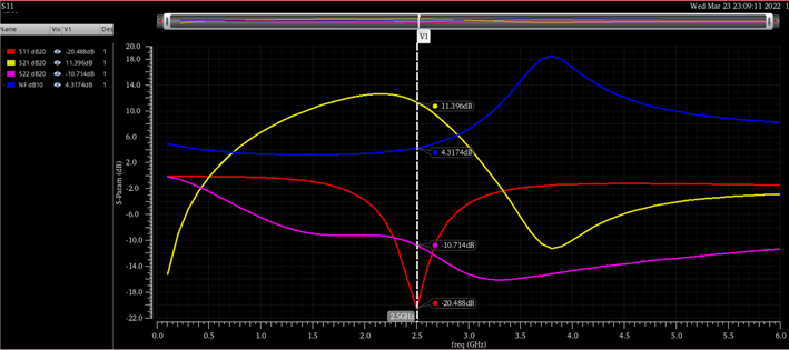
Here is the schematics, the testbench and some results (s parameters analysis). I would like to know if there is a way of increasing the gain and decreasing the noise factor of my amplifier. Thank you.

[![enter image description here][1]][1]

So in case values are not visible this LNA is made of:

  • An input resonance between a 4.7 nH inductor and a 400 nF capacitor -> tunes it to 2.5 GHz.
  • A biasing resistor of 6.67 kohm. VGG is obtained as half of VDD by those rightmost ressitors of also 6.67 kohm.
  • A MOS transistor with L=0.35u and W=200u.
  • A load inductor of 4.7 nH.
  • A DC decoupling capacitor of 5 pF.

[![enter image description here][2]][2]

On the testbench the 3.3V source is visible. The inductors of 500pH are to simulate pads inductance. The capacitor of 1mF is just for DC decoupling when obtaining the DC bias point

enter image description here

Simulations:

  • S11 (red curve) gives if the amplifier is matched or not (it it is under -15 dB) -> -20.488 dB

  • S21 (yellow curve) gives the gain. If it is above 10.5 dB is good -> 11.396 dB (good but I wish it was better).

  • S22 (pink curve) below 0 dB to gurantee stability (positive real part impedance) -> it checks out

  • Noise Figure (blue curve) just a little above 3 dB -> this is where things are a bit bad with a noise figure of 4.3 dB

I also see a strange zone where NF and S21 vary a lot around 4 GHz? Why is that?

Any opinions?

Thank you!

\$\endgroup\$
2
  • \$\begingroup\$ I'd like to see design work product. I don't go to prototype or simulator until I already know what to expect (and why.) What was your design procedure to optimize S/N? Should I see something with \$\sqrt{g_m}\$? What's \$f_T\$ for the FET? \$\endgroup\$
    – jonk
    Commented Mar 24, 2022 at 2:27
  • \$\begingroup\$ Run a noise summary (slide 7 of this document) at a frequency spot of 2.5 GHz. What are the main contributors? \$\endgroup\$
    – nanofarad
    Commented Mar 24, 2022 at 2:55

1 Answer 1

1
\$\begingroup\$

I also see a strange zone where NF and S21 vary a lot around 4 GHz? Why is that?

This could be the series resonance of the input inductor and the parasitic capacitance of the MOSFET. At this frequency the input impedance of the LNA is at a minimum and the input signal is attenuated heavily -> S21 below 0 dB. Attenuating the input signal also leads to a higher noise figure because the noise contributed by the LNA stays about the same but the signal power is lower.

Assuming you want to keep using the CE-topology, there are a few things to try to increase gain and lower the noise figure.

  1. Make sure you are biasing the MOSFET at the minimum noise current density which is likely to be about 0.15 mA/µm (drain current / gate width) but could be up to 0.3 mA/µm. You can run simulations to find out exactly. enter image description here

Source: High-Frequency Integrated Circuits, S. Voinigescu

  1. Adjust the transistor width to improve matching to the 50 Ohm input impedance while keeping the minimum noise current density the same (so adjusting biasing at the same time as transistor scaling).

  2. Adjust input matching components to improve S11.

  3. Increasing the load inductor would increase gain but might also changes input and output matching.

While step 1 should be straight forward, there might be simulation tools/testbenches that can assist with the other steps. Given the limited parameters that can be changed, you could also try on your own to get a feel for what each slight parameter change does and design in an iterative way.

I would also recommend looking into the book High-Frequency Integrated Circuits by S. Voinigescu which explains the process in much more detail.

\$\endgroup\$
4
  • \$\begingroup\$ Oh I have just realized I don't have a good output matching as S22 is not below -15 dB, unlike S11. I think that is what I have to tackle first. Any tips. I've tried to increase the output inductor to 9 nH but that seems to make things worst. Tecnhology does not alow me to increase the capacitor over 5 pF. \$\endgroup\$ Commented Mar 24, 2022 at 17:06
  • \$\begingroup\$ Transistor scaling will also affect impedance matching. You will probably need to do multiple design iterations overall. \$\endgroup\$ Commented Mar 24, 2022 at 19:21
  • \$\begingroup\$ I'm in the maximum transistor width already. I am really lost have done more than 50 simulations already :/ \$\endgroup\$ Commented Mar 24, 2022 at 19:27
  • \$\begingroup\$ what is your opinion on decreasing the inductor size? \$\endgroup\$ Commented Mar 24, 2022 at 19:33

Your Answer

By clicking “Post Your Answer”, you agree to our terms of service and acknowledge you have read our privacy policy.

Not the answer you're looking for? Browse other questions tagged or ask your own question.