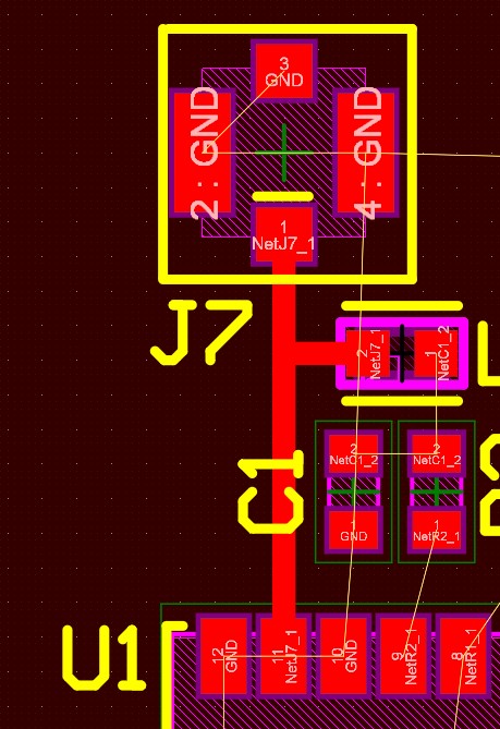
I'm working on a 4 layer board (signal, GND, PWR, signal). I have a NEO-M8P GPS module and the Hardware integration manual says to connect the antenna with a 50 ohms impedance trace to the connector which I did. I've also been reading and watching videos for best practices routing the 4 layer board and I came across "Via Stitching & Via Shielding". There are lots on info about these two subjects. The picture below shows the trace from the GPS antenna pin (U1 pin 11) to the connector (J7). The trace to the side is an inductor needed for active antenna support (Figure 8 in the Hardware integration manual). There is an MCU in the middle of the PCB and a few sensors around it. There is really nothing high speed. The GPS parts are on the edge of the PCB. I'm wondering if I need to add Via Shielding to the GPS antenna trace?
1 Answer
Adding via stitching as shown in the Altium article makes that a coplanar waveguide which will alter the impedance of the trace unless you make the necessary corrections. Doing so creates issues in maintaining impedance when you consider the physical interference from the inductor. If you're worried about interference, you can shorten up the antenna trace quite a bit or add a shield around the sensitive area as done in many designs.
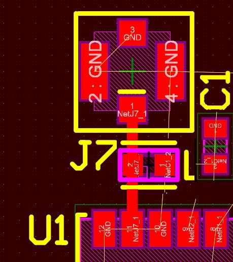
What would help is moving the inductor so the inductor pad is directly over the GPS antenna trace. This minimizes the stub caused by the trace to the inductor which causes an impedance bump. You may want to move C1 which allows shortening of the antenna trace.


