2
\$\begingroup\$

current regulator circuit

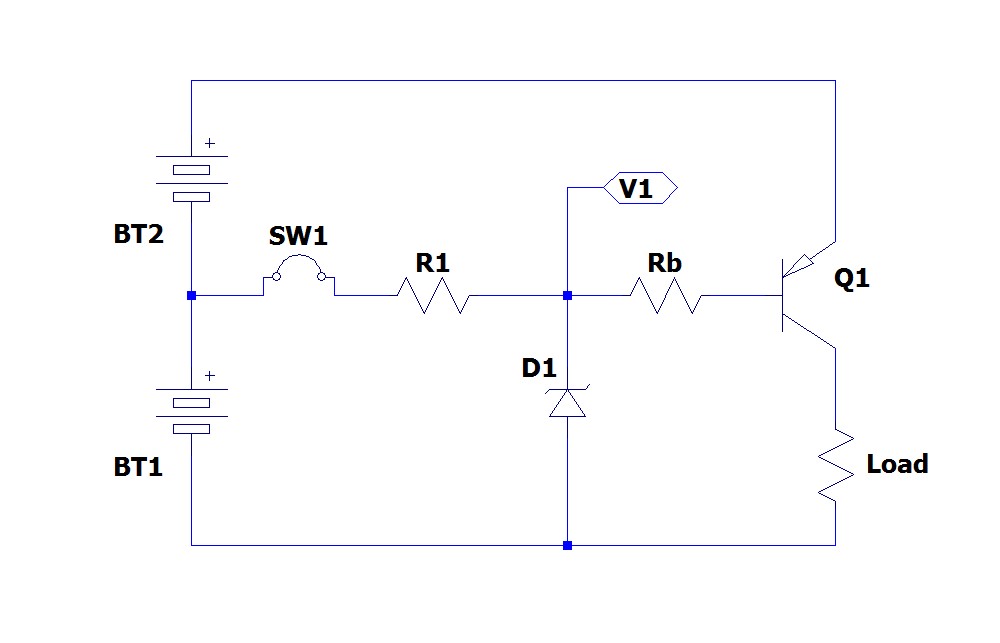
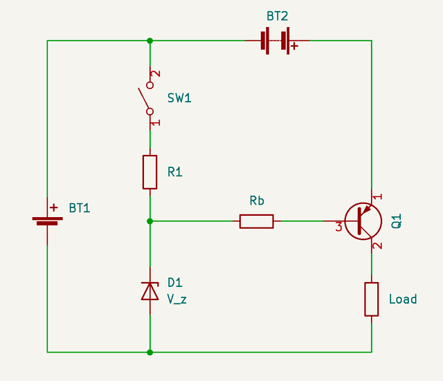
I want to build a circuit that supplies constant current to my load.

In theory, the PNP transistor is in its active state when the switch is closed. D1 and R1 will reach a stable point on the Zener diode's characteristic curve (e.g. voltage \$V_1\$, current \$I_1\$ across D1.)

This will supply a constant current (\$I_b\$) to the base, which will fix the emitter-collector current to a \$\beta\$ multiple of \$I_b\$ over a wide range of voltages. The reason I'm using a Zener diode is because BT1's voltage drops over time which will affect \$I_b\$.

I predict the current to the load to be: $$ I_{\text{Load}} = \beta \frac{V_1 - V_{\text{BC}} - V_{\text{Load}}}{R_b} $$

Can the Zener diode maintain a stable base current and regulate load current as expected?

Is it sufficient to determine \$V_1\$ by load line method using only BT1, R1 and D1, ignoring the rest of the circuit?

\$\endgroup\$
10
  • 3
    \$\begingroup\$ The temperature coefficients of the zener and Vbe, as well as the part-to-part variation in beta and several other factors make this idea impractical. A better alternative would be a current mirror, and better yet an op-amp/bjt or FET current source. \$\endgroup\$
    – John D
    Commented Jul 7, 2022 at 16:44
  • \$\begingroup\$ If you want a single BJT stage with a collector current as constant as possible you should be aware that the BJT is a voltage-driven device. Therefore, use a low-resistive voltage devider at the base (advantage: Base voltage nearly independent on the base current and its pretty large uncertainty) and use a current stabilizing emitter esistor RE. \$\endgroup\$
    – LvW
    Commented Jul 7, 2022 at 16:59
  • \$\begingroup\$ @JohnD I read that beta can increase with temperature: electronics.stackexchange.com/questions/490868/…, but there seems to be a way to counteract it by adding an ohmic load to the emitter. The resistor-zener series appears to be a standard circuit used for voltage regulation. As I see it, the zener diode circuit and transistor circuit work fine on their own. Is putting them together really so impractical? \$\endgroup\$
    – coulombs
    Commented Jul 7, 2022 at 18:06
  • \$\begingroup\$ @coulombs With an emitter degeneration resistor you could improve the circuit. Since you haven't added any performance specs or requirements it's hard to comment beyond that. The early effect, the previously mentioned tempcos, and part-to-part variation if you're building more than one of these will all impact performance. \$\endgroup\$
    – John D
    Commented Jul 7, 2022 at 18:47
  • 2
    \$\begingroup\$ Why two sources? \$\endgroup\$
    – DKNguyen
    Commented Jul 7, 2022 at 20:10

4 Answers 4

2
\$\begingroup\$

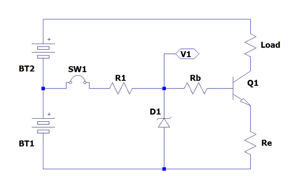
This is your circuit redrawn. enter image description here It appears that you are trying to feed the base of the transistor with a Zener regulated voltage, the problem is that this voltage is referenced to the collector of the transistor through the variable load, when it should be referenced to the emitter through a fixed resistance.

In order to do that you could swap the emitter and collector, but to do that and keep the diode and battery polarities the same you would need to switch to an NPN transistor. You would also need to add an emitter resistor and move the load. Here is the circuit with those changes: enter image description here This will make it regulate the current much better than the original did (which was pretty much not at all) but it's got room for improvement.

A few ideas:

  • Do away with one battery and connect R1 to the positive of the remaining one.
  • The Zener can be replaced with a regular diode or LED, but with the anode and cathode swapped.
  • You could also use a better CCS topology, such as a two transistor CSS.
  • If you still wanted to use a PNP transistor you would swap the polarities of the batteries and diode.

There are plenty of constant current source designs out there, some use a Zener, some other types of diodes, some use another transistor. You can also control the current to a load by adding a current sense resistor and using an opamp to sense the voltage across it and drive a pass transistor. Do a bit of research into current sources/sinks and current sensing, that should lead you to some better ideas.

\$\endgroup\$
3
  • \$\begingroup\$ The denominator in my equation is the resistance of the base resistor, not the resistance of the load, so our equations are different. Also, I should mention that my load is non-ohmic. I suspect that there might be some other mistake in my equation. Thanks for helping me check. \$\endgroup\$
    – coulombs
    Commented Jul 7, 2022 at 17:47
  • \$\begingroup\$ The circuit diagram you made is different from the circuit I am asking about. Please refer to my original diagram and question. I appreciate your help, but you won't be able to provide a relevant answer unless you understand the circuit. \$\endgroup\$
    – coulombs
    Commented Jul 7, 2022 at 20:50
  • \$\begingroup\$ @Godjihyo: Schematic diagrams are usually drawn with positive power supply at the top and ground at the bottom. I think non-ohmic refers to a non-linear load, like an incandescent lamp or diode, which do not have a fixed E/I relationship. \$\endgroup\$
    – PStechPaul
    Commented Jul 9, 2022 at 4:36
1
\$\begingroup\$

Can the Zener diode maintain a stable base current and regulate load current as expected?

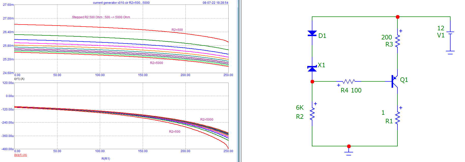
The answer is "no". Zener can only fix the Base voltage.
If you give the value of BT1 and BT2, it is possible to show what one can expect ...

If you move the Zener, then one can expect a "constant" current.
See this example.

enter image description here

\$\endgroup\$
1
\$\begingroup\$

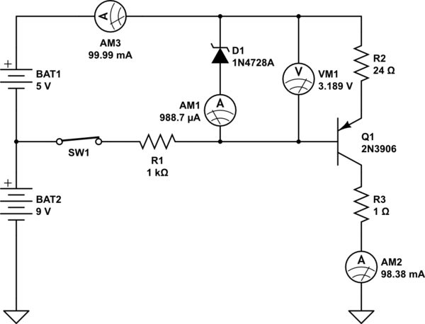
To convert base voltage to a current, you need a resistor in the emitter circuit. As follows:
schematic

simulate this circuit – Schematic created using CircuitLab

No need for a base resistor.

R1 is the load for the 3.3V Zener diode D1, and the base load as well. R2 sets the current. R3 is the load.

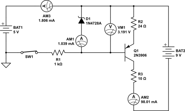
There's no need to split the supply voltages, although for now let's keep the split. The load current flows through BAT1. You probably want the load current flowing through BAT2 only:
schematic

simulate this circuit

Now, the problem is that the Zener current through D1 depends on Q1's beta: the lower the beta, the more current flows out of the base, and less through D1. We should stabilize the current through D1.

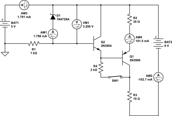
We can add Q2 to decouple the Zener voltage from Q1's base. Even with beta variations, the base current of Q2 through D1 is so small as not to destabilize the Zener voltage much.
schematic

simulate this circuit

R4+SW1 can be returned to the load, or to BAT2's negative terminal.

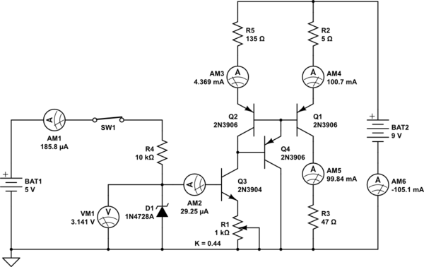
But now SW1 doesn't turn off the Zener, and BAT1 is wasting power. Instead, we can use a scaled current mirror:
schematic

simulate this circuit

R5/R2 set the current ratio between Q1/Q2. R1 sets the reference current, based on the Zener voltage buffered by Q3. Q4 buffers Q1's base current and improves the accuracy of the current source. Q1+Q2 must be in thermal contact. Ideally, both would be identical medium-power devices, mounted nearby on the same heatsink. If the dissipation is low, the current sink can be quite small.

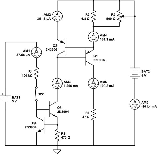
Now, instead of using the Zener voltage, we can use the B-E voltage of a bipolar transistor Q2, operating under fixed-current conditions:
schematic

simulate this circuit

R2||R9 is the current shunt and also sets the current through Q1. The voltage across the shunt is compared against Q2's VBE. Q2 closes the negative feedback loop and robs Q1's base current as needed to maintain a fixed voltage across the current shunt.

A similar current stabilization loop is implemented by Q3-Q4, to stabilize the collector current of Q2, improving the accuracy of the primary current control loop.

In the two foregoing circuits, BAT1 is optional, and the circuit it feeds can be connected to BAT2 instead.

The approximately 0.7V across the current shunt may not be acceptable if the circuit should operate down to a minimal voltage on BAT2 as it discharges.

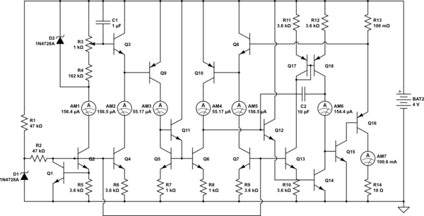
A low resistance current shunt can be used if we implement an op-amp:
schematic

simulate this circuit

The circuit above operates with current stabilized to about 0.1% from 5V to 30V, and within 1% down to about 3.7V. Transistor matching should be unnecessary, although all NPN and PNP types should be respectively identical, with exception of Q16.

D1 stabilizes the current reference Q1-Q2. The stabilized current is then used to establish the Zener current through D2. R3-R4 is the reference voltage divider, establishing the current setpoint across the shunt R13. The reference current is used to bias the input stages of the differential amplifier, as well as a part of the output stage. To improve performance with discrete components, the current mirrors have strong emitter degeneration. The circuit is quite insensitive to slow changes in the load impedance.

\$\endgroup\$
1
  • \$\begingroup\$ Very sophisticated design... Well done! \$\endgroup\$ Commented Jul 11, 2022 at 20:04
0
\$\begingroup\$

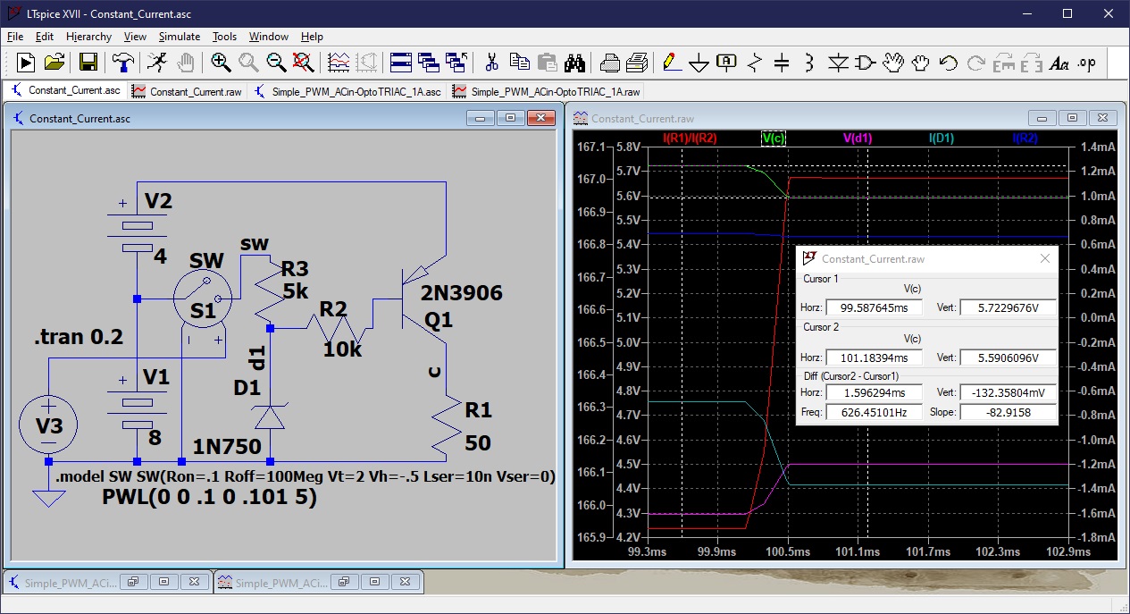
I'm not sure what is being attempted in @coulomb's circuit, but the zener will (to some extent) regulate base current and thus also collector current when the switch is closed. However, the only thing that does is drive more current through the zener diode, which will cause its voltage to rise slightly. The collector current follows base current according to beta, but that can vary considerably between devices, as well as temperature, voltage, and current. This might show some of the circuit's operation:

Circuit simulation

\$\endgroup\$

Your Answer

By clicking “Post Your Answer”, you agree to our terms of service and acknowledge you have read our privacy policy.

Not the answer you're looking for? Browse other questions tagged or ask your own question.