3
\$\begingroup\$

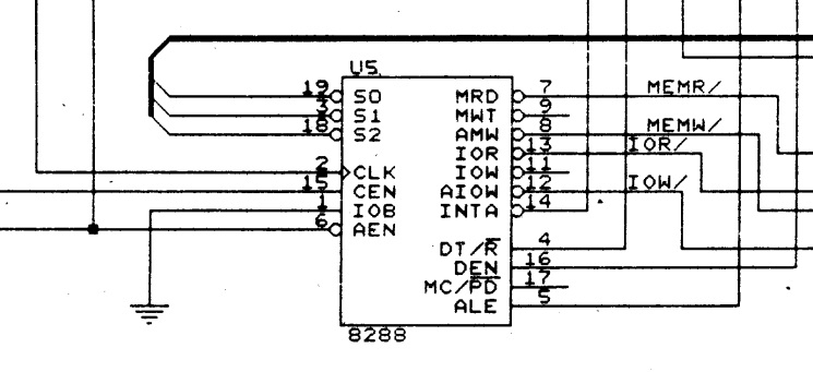
I'm trying to dig into the early IBM PC's arhictecture, and got stuck with one thing that is not really clear to me. Every PC XT schematic I saw, including the original one from "IBM 5160 Technical Reference" use AMW and AIOW (sometimes also referred as AMWC and AIOWC) active low signals of the 8288 bus controller as their memory/IO write strobes. For example, this schematic:

8288 bus controller of IBM PC XT

As you can see, normal write (MWT and IOW) signals are left unconnected here. And, as far as I understand, target memory/IO device uses AMW/AIOW signal, or, to be more precise its leading edge (high-to-low) transition as a command to read the data from the data bus. However 8088/8086 datasheets say this:

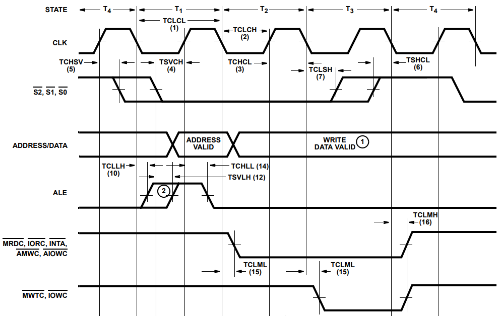
The 82C88 provides two types of write strobes, normal and advanced, to be applied as required. The normal write strobes have data valid at the leading edge of write. The advanced write strobes have the same timing as read strobes, and hence, data is not valid at the leading edge of write.

This sounds confusing, because this means that any device that uses advanced write strobes of the 8288 bus controller is going to read garbase, because CPU has not yet provided any meaningful data to the bus. So, I am wondering how it still works that way in the IBM PC XT, and where I am wrong in my conclusions?

What is the purpose of these advanced write signals, and why PC XT designers used them instead of normal write strobes, which would have data perfectly valid at their leading edge?

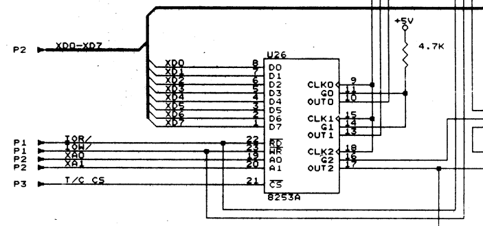
UPDATE: At first I accepted @Kuba hasn't forgotten Monica's answer, but then went to check the schematics again, and it seems that target devices actually use leading (high-to-low) transition to read the data from the bus. Like 8253A PIT does here:

PIT connection

IOW is connected to the WR input of 8253A, its WR input is active low, and 8253A datasheet says:

8253A WR signal description

So, my above questions still remain relevant. Isn't 8253A going to read anything but the real data in this case? Because at this point, when advanced write strobe goes low, CPU is not actually outputting data on the bus.

\$\endgroup\$
8
  • 1
    \$\begingroup\$ Welcome! You may be able to find folks with better context regarding this at Retrocomputing. (not voting to close because this question is still on-topic here to the best of my understanding) \$\endgroup\$
    – nanofarad
    Commented Jul 15, 2022 at 22:24
  • 1
    \$\begingroup\$ It's an active low signal, not edge dependent. Allows more time to meet timing for peripherals without inserting wait states. \$\endgroup\$ Commented Jul 16, 2022 at 2:27
  • 2
    \$\begingroup\$ There's really no need to have data valid at the leading edge of write strobe. It just has to be valid with enough setup time to the trailing edge of write strobe. \$\endgroup\$
    – Dave Tweed
    Commented Jul 16, 2022 at 4:16
  • 1
    \$\begingroup\$ Even with your update, it still doesn't mean that the 8253 is using the data at the leading edge. The data just needs to become valid before its WR- signal goes high again. \$\endgroup\$
    – Dave Tweed
    Commented Jul 16, 2022 at 13:43
  • 1
    \$\begingroup\$ It's true that if the slave device uses transparent latches, you might see glitches on the outputs as the bus data settles during the write pulse. For example, if you're writing to an SRAM, it doesn't mattter if the SRAM cell switches a couple of times during the write cycle, as long as it's in the correct state after the cycle is over. But most I/O devices use edge-triggered flip-flops, triggered at the trailing edge of the write pulse. This is where the setup time requirements for the device come from. \$\endgroup\$
    – Dave Tweed
    Commented Jul 16, 2022 at 13:51

2 Answers 2

4
\$\begingroup\$

This sounds confusing, because this means that any device that uses advanced write strobes of the 8288 bus controller is going to read garbase, because CPU has not yet provided any meaningful data to the bus.

That would be true if the devices expected the data to be valid at the leading edge of the strobe. That's not the case. The leading edge is there to trigger address decoders and other combinatorial circuits. They get a chance to settle early enough for when the trailing edge of the strobe comes, the data has been valid long enough to satisfy the setup times.

The whole reason for the bus controller providing the advance outputs is to allow typical decoder/gating circuits to act before the write is over.

\$\endgroup\$
1
  • \$\begingroup\$ Seems like it is not the case with the trailing edge, I've updated my question. \$\endgroup\$
    – Linol
    Commented Jul 16, 2022 at 11:52
1
\$\begingroup\$

From Renesas 82C88 CMOS Bus Controller

Command Outputs

The advanced write commands are made available to initiate write procedures early in the machine cycle. This signal can be used to prevent the processor from entering an unnecessary wait state.

enter image description here

The standard CPU cycle takes 4 clock cycles. 1st clock cycle Address and ALE.

The standard write cycle is just 1 clock. Advanced is 2 clocks. The signals are active low. Address/Data is just for reference only.

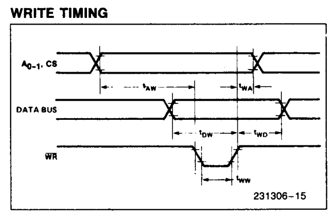
From 8253 data sheet enter image description here

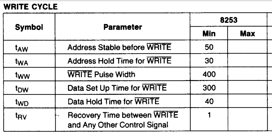
enter image description here

Notice there are no clocks here. The timings for the write signal are referenced to rising edge of write signal. The minimum write pulse \$t_{WW}\$ is 400ns, but the minimum data set up for write \$t_{DW}\$ is 300ns and the data hold time \$t_{WD}\$ is 40ns.

This means that the write data does not have to be available at the start of the write signal, but must be available 300ns before the rising edge of the write signal. The write signal is active low but data gets latched on rising edge.

Now the advanced write signals are used to allow for more time to complete the write or external circuitry will have to insert wait states. I/O devices were slow so wait states had to be inserted.

8Mhz 82C88 part means each clock cycle is 125ns. Even using advanced timing, the write pulse is only 250ns, which is not compatible with a 400ns 8253 write, so 2 wait states must be inserted (375ns < 400ns, so write is 500ns long). Wait states delay processor by additional clock signals to make processor compatible with slower devices.

OTTOMH The original 8088 4.77MHz IBM PC had 4 wait states for I/O and 2 wait states for memory.

\$\endgroup\$
2
  • \$\begingroup\$ I am ashamed I did not pay attention that setup and hold times were given relative to the rising edge of WRITE. Now it is clear to me why "This [advanced] signal can be used to prevent the processor from entering an unnecessary wait state.", because normal ones which are shorter, are going to give less setup time for a target device. \$\endgroup\$
    – Linol
    Commented Jul 17, 2022 at 21:15
  • 1
    \$\begingroup\$ Yes. Different devices from different manufacturers and families had different setup and hold times. Advanced just allows more time, hence usage in IBM PC. \$\endgroup\$ Commented Jul 18, 2022 at 2:54

Your Answer

By clicking “Post Your Answer”, you agree to our terms of service and acknowledge you have read our privacy policy.

Not the answer you're looking for? Browse other questions tagged or ask your own question.