0
\$\begingroup\$

I have question regarding SPI termination when using three-state buffers:

  1. Do we need termination resistor from master to three-state buffers (since ICs are very close)
  2. If we do, then do calculate the trace impedance from three-state buffer to master or slave to master.
  3. How MISO where you put termination resistor (close to slave or buffer)
  4. Do we even need termination resistor since max trace space is around 20 cm.

Let assume we have below setup which we have two 3.3 V slave. Note: OE is enabled for all channels. (74LVC126)
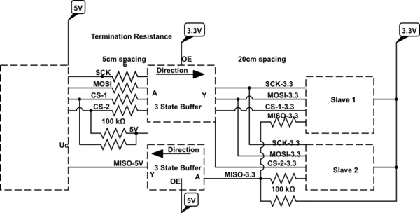
schematic

simulate this circuit – Schematic created using CircuitLab

Please let me know if drawing is not clear or you need more information.

Base on Jens answer

schematic

simulate this circuit

\$\endgroup\$
4
  • \$\begingroup\$ Why do you use 3 state buffers at all? Your circuit does not contain any 3 state control logic (OE) anyway. \$\endgroup\$
    – Jens
    Commented Jul 20, 2022 at 2:27
  • \$\begingroup\$ @Jens yes it does I didnt show in schematic, I only show that all of is enable( I will go head and added) \$\endgroup\$
    – Shahreza
    Commented Jul 20, 2022 at 2:28
  • \$\begingroup\$ Can you edit your question and add the 3-state buffer part number. Are these buffers or just voltage translators? Thanks. \$\endgroup\$
    – TonyM
    Commented Jul 20, 2022 at 8:04
  • \$\begingroup\$ @TonyM I am using 74LVC126 \$\endgroup\$
    – Shahreza
    Commented Jul 20, 2022 at 13:36

1 Answer 1

2
\$\begingroup\$

You obviously don't use the third high impedance state of the drivers, they are just used as level shifters.

During reset or firmware update the MCU may have undefined voltages at the SPI pins. Therefore I recommend to add pullup resistors at least to the CS-x signals. If they both are accidentially low, the two slaves will drive the same MISO line. This must be avoided.

When the high impedance feature of the driver is used, you need these CS pullup resistors on the slave side as well. I prefer a 100 kohm resistor at the MISO line to avoid floating voltages if no slave is selected.

20 cm trace length is significant, if you feed these lines with series resistors of 33-100 ohm you will have less EMI problems and lower ringing. At the receiver end you can design in an optional pullup resistor just in case.

For very high frequency SPI channels like SD cards, things are different. In my experience a proper termination (e.g. 330 ohm) is necessary at this distance.

\$\endgroup\$
5
  • \$\begingroup\$ Thanks for the answer. I update schematic based on your comment, but I have some questions: 1. CS pullup do you put only on slave side or should I put it on uC side before buffer or both 2. Do I put MISO Pull up on both salve side (After buffer) 3.Terminating resistor where do I put it on SCK,MOSI close uC before buffer or after buffer or both – \$\endgroup\$
    – Shahreza
    Commented Jul 20, 2022 at 14:06
  • \$\begingroup\$ @Shahreza Move the 4 series resistors to the right (output) side of the buffer and everything is fine. \$\endgroup\$
    – Jens
    Commented Jul 20, 2022 at 14:47
  • \$\begingroup\$ Thanks for the answer. \$\endgroup\$
    – Shahreza
    Commented Jul 20, 2022 at 15:18
  • \$\begingroup\$ @Shahreza, please can you edit your question to add another copy of the schematic but with the resistor changes that you have agreed with Jens. That way, future question readers can find the answer without hunting through the comments here. Thanks. \$\endgroup\$
    – TonyM
    Commented Jul 20, 2022 at 17:43
  • \$\begingroup\$ @TonyM I just updated the schematic. \$\endgroup\$
    – Shahreza
    Commented Jul 20, 2022 at 18:25

Your Answer

By clicking “Post Your Answer”, you agree to our terms of service and acknowledge you have read our privacy policy.

Not the answer you're looking for? Browse other questions tagged or ask your own question.