2
\$\begingroup\$

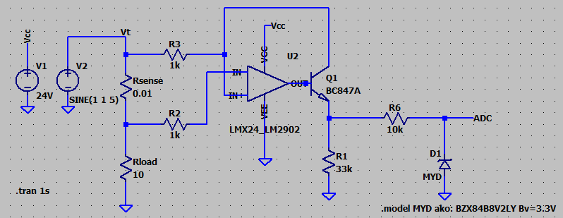
I would like to use the schematic below to measure the output current of a buck converter (0-10 A) and convert it to a voltage of 0-3.3 V which is read by a microcontroller. During startup I sometimes run into the problem which I have simulated below.

When the voltage at the sense resistor drops to near 0 V, the op-amp (LM324) output jumps to the supply voltage of 24 V and stays there. Since the input voltage is close to 0 V I would expect some undesired behaviour like this, but I don't understand why it does not 'recover'? What would be the best way to resolve this?

enter image description here

enter image description here

\$\endgroup\$
11
  • \$\begingroup\$ Two things to consider: what is the Voh and Vol of the LM324 (how close can the outputs get to the power rails?) And what is the intrinsic junction capacitance of the BZX8VB8V2LY BZX84-B8V2? Likely 450pF. When charged, how is this junction capacitance discharged? \$\endgroup\$
    – rdtsc
    Commented Sep 1, 2022 at 19:34
  • 2
    \$\begingroup\$ Do you have it wired for positive feedback instead of negative? It's difficult to tell the input pins apart. \$\endgroup\$
    – Null
    Commented Sep 1, 2022 at 19:36
  • 2
    \$\begingroup\$ That circuit cannot do what you want. You are trying to read 10A through a 10 mOhm resistor, which is 100 mV, with a common mode voltage that varies from zero to probably 10 volts or more, and you need a gain of 30. If you can put the sense resistor on the low side, a simple non-inverting amplifier will work. Otherwise you really need a high side current monitor, best accomplished with an appropriate IC. \$\endgroup\$
    – PStechPaul
    Commented Sep 1, 2022 at 19:41
  • \$\begingroup\$ Is it possible that you're forward-biasing the base-collector junction in Q1, resulting in accidental positive feedback? \$\endgroup\$
    – brhans
    Commented Sep 1, 2022 at 20:58
  • 1
    \$\begingroup\$ I think it happens before that. The B-C junction getting forward-biased causes the positive feedback which makes the output jump up to Vcc. Most of the time, your opamp's negative feedback comes from Q1 conducting and drawing current away from the opamp's non-inverting input through R1 in order to get the non-inverting input to almost the same voltage level as the inverting input. But that feedback mechanism will only really work as long as the opamp's output stays below the voltage at the non-inverting input - and the lower your input voltage the closer you get to where things go wrong ... \$\endgroup\$
    – brhans
    Commented Sep 2, 2022 at 18:45

4 Answers 4

2
\$\begingroup\$

Looking at your schematic, I can't see what Q1 is supposed to do, but it seems as if the inverting nature of Q1 should make the loop feedback negative.

However, one thing that stands out is that it is easily possible for Q1's base potential (the op-amp output) to exceed its collector potential, and forward bias the base-collector junction. If that happens, then collector potential will "follow" the base, and feedback becomes positive.

I think that's why your op-amp locks up in a high state.

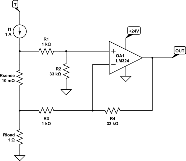
Since I don't know what Q1 is supposed to achieve here, the best answer I can give you is a suggestion which wouldn't suffer from this problem, but doesn't use Q1:

schematic

simulate this circuit – Schematic created using CircuitLab

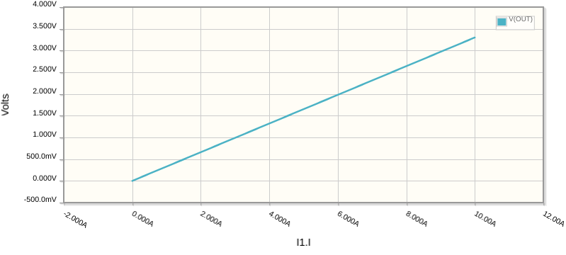
That's just a basic differential amplifier, with gain of 33. It behaves like this:

enter image description here

\$\endgroup\$
1
\$\begingroup\$

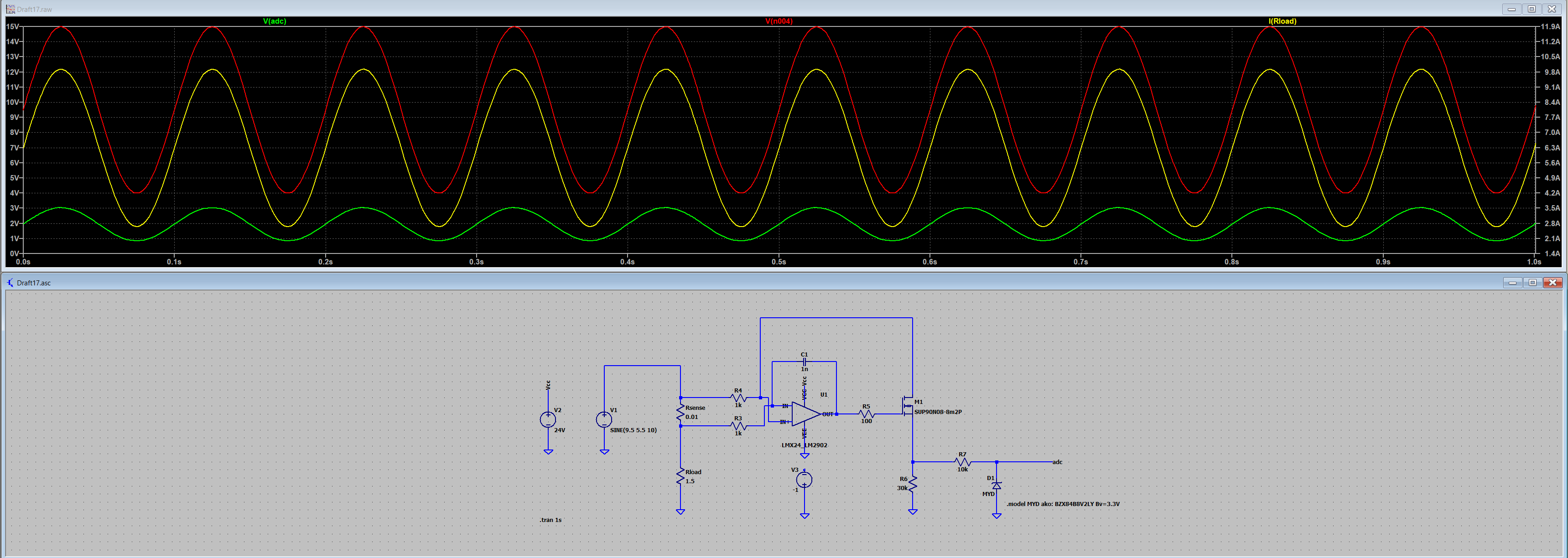
Thanks all for your comments/anwsers! I seem to have resolved my problem by replacing Q1 with a mosfet and I also added some capacitive feedback (see below). I updated my prototyping board with these changes as well and the microcontroller indeed seems to return the actual output current of my buck converter.

enter image description here

\$\endgroup\$
3
  • \$\begingroup\$ Yep - by using a MOSFET there you'll never run into the problem in your original circuit where the forward-biased BC junction gives you runaway positive feedback. \$\endgroup\$
    – brhans
    Commented Sep 2, 2022 at 19:53
  • \$\begingroup\$ I don't think that will work. You have the variable voltage source connected to the drain of the MOSFET, through a 1k resistor R4, and the low side of the shunt connects to the Op-amp inverting input through R3. The output of the op-amp drives the gate of the MOSFET, but it will always be fully ON, and you will be reading the voltage on Rload. However, that would be a 5.5V sine wave on 9.5V offset which is V(n004). So I don't see how you got that. \$\endgroup\$
    – PStechPaul
    Commented Sep 3, 2022 at 7:22
  • \$\begingroup\$ OK, I simulated it, and got the same results you did. However, the gain (30) seems to be related to the ratio of R4 and R6. And it becomes unstable and oscillates if I change R4 from 1k to 2k. It also oscillates with offset 5V and 3V sine wave (or even 0.5V). It seems an offset of 6 or 7 volts or less causes instability. \$\endgroup\$
    – PStechPaul
    Commented Sep 3, 2022 at 8:35
1
\$\begingroup\$

If you must use a high-side current monitor, you could try a circuit like the one I have simulated below. It won't be accurate for input voltages near zero, but it is within 1% from 5 V to 35 V, for which I use a 15 V sine wave with 20 V DC offset.

The output voltage between R2 and R4 (a and b) equals the voltage on the 100 mΩ shunt R5 (Vin and Vout). It also works with a 10 mΩ shunt, but the error increases to about 5%-8% for common-mode voltages of less than 6 V. If you do this, you may need to tweak the values to get the performance you desire, and you will still need an amplifier with a gain of 30 to get the required signal to your ADC.
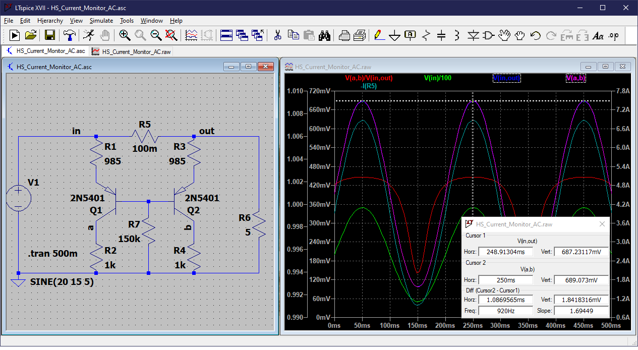
High Side Current Monitor

I was able to achieve about 1% error down to a range of 1 V to 39 V with a 10 mΩ shunt by using 975 Ω for R1 and R3, and 1 MΩ for R7.

I simulated the OP's circuit using an AD820 and 2N2222, and the output was basically slammed to the 24 V Vcc rail.

OK. Here is a practical circuit, although it also has some unwanted behavior, which might be due to the simulator. For one thing, the voltage across the shunt resistor should not be distorted (or go below zero).
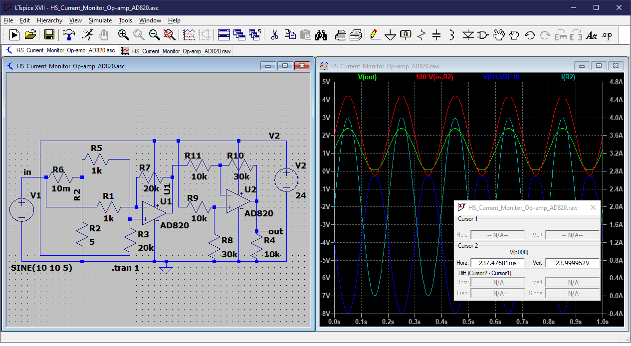
High Side Current Monitor with two AD820 Op-amps

I was not really satisfied with the last circuit, so I came up with the following, using a current mirror and a single op-amp. I also used a step function to test it for a range of power supply voltages. This still needs very close matching of the differential amplifier resistors:
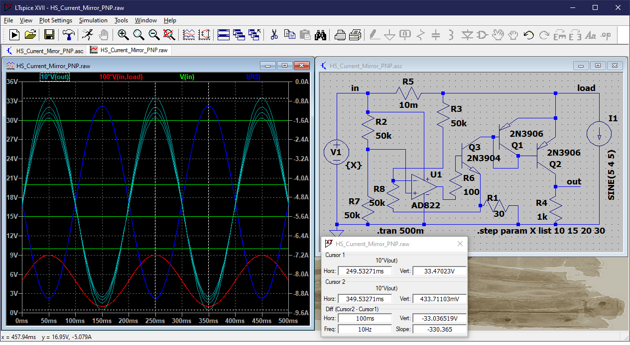
High Side Current Mirror PNP

I simulated the circuit provided by @emdura, and found problems with it. However, I used most of the same components and made some changes that work properly. The source follower MOSFET is not really necessary, but is provided in case higher output current is desired. At least this design does not depend on the value of the load resistor.
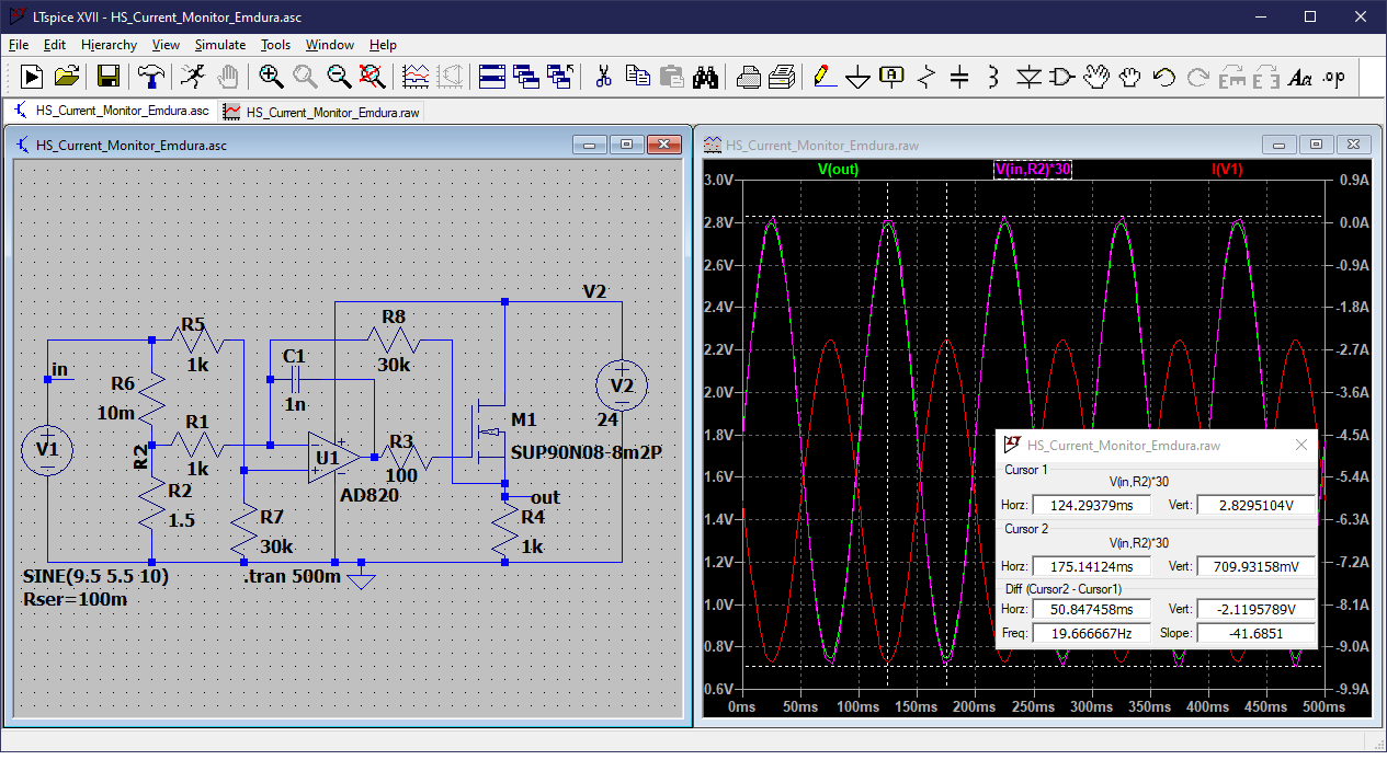
High Side Current Monitor @emdura

\$\endgroup\$
2
  • \$\begingroup\$ thank you for your elaborate anwser, for now I have resolved my problem in a different way, but I might still try out your circuit as well \$\endgroup\$
    – emdura
    Commented Sep 2, 2022 at 14:41
  • \$\begingroup\$ I discovered that my circuit is extremely sensitive to the exact values and ratios of the resistors. And the transistors must be very well matched. So probably not all that practical. \$\endgroup\$
    – PStechPaul
    Commented Sep 3, 2022 at 3:39
0
\$\begingroup\$

Real op-amps have offset. You'll have to add the worst-case offset to the input plus a small margin. Then it won't saturate. But that will require a slightly different design.

You have two choices:

  1. Use a purpose-made high sensing current shunt amplifier. Those usually are easy to interface straight to 3.3V ADC inputs.

    The upside: one chip. The downside: there are no industry standard pinouts/specs, so if the part is not available, you either have to wait or redesign.

  2. Use a discrete design.

    The upside: if you can't buy the parts, the world is ending and you don't need to worry about it anymore :) The downside: more drift, but performance can be improved by using better op-amps in the same package.

There isn't much to applying high-side sensors if you follow their datasheet and/or app notes. So we'll explore a discrete design.

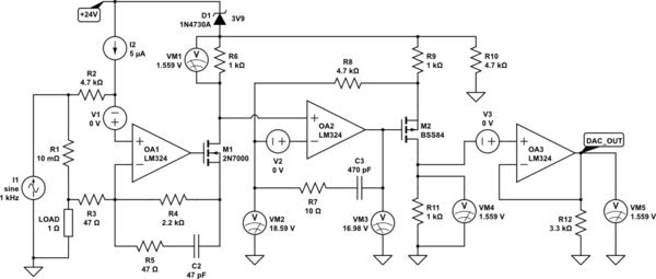
OA1 copies scaled version of the input current onto R6. I2 driving R2 adds an offset voltage that compensates for worst-case offsets in OA1 and elsewhere in the system. I2 would be e.g. an LM334, or any other current source with compliance voltage range from 10 to 25V.

OA2 mirrors the current from R6 onto R9 and R11.

OA3 buffers the output voltage.

D1-R10 establish about 4V of headroom from the top rail, so that the op-amp inputs are within their common-mode range.

V1, V2 and V3 are used to model op-amp offset voltages.

schematic

simulate this circuit – Schematic created using CircuitLab

The output voltage waveform is shown below. The load is driven with a 1kHz 0-10A sine wave current waveform. The top and bottom curves are for the worst case input offset voltage in OA1, since that offset dwarfs the others.

enter image description here

This circuit always recovers from disturbances even if they saturate the outputs.

To improve performance, use op-amps with more gain, better linearity and offset drift. The requirements for the op-amps are modest:

  • OA1, OA2
    1. Input common mode range from (V-) to (V+)-2V.
    2. Output voltage range: (V-)+2V to (V+)-2V.
  • OA3 - if powered from 24V (eg LM324):
    1. Input common mode range from (V-) to (V+)-2V.
    2. Output voltage range: (V-) to (V+)-5V.
  • OA3 - if powered from 5V:
    1. Input common mode range: (V-) to (V+)-2V.
    2. Output voltage range: (V-) to (V+)-2V.
  • OA3 - if powered from 3.3V:
    1. Input common mode range: rail-to-rail
    2. Output voltage range: rail-to-rail

R12 ensures LM324 performance with output close to 0V. It should be removed for other op-amp families, unless the datasheet dictates otherwise.

\$\endgroup\$
1
  • \$\begingroup\$ Thank you for your elaborate anwser, for now I have resolved my problem in a different way, but I might still try out your circuit as well \$\endgroup\$
    – emdura
    Commented Sep 2, 2022 at 14:42

Your Answer

By clicking “Post Your Answer”, you agree to our terms of service and acknowledge you have read our privacy policy.

Not the answer you're looking for? Browse other questions tagged or ask your own question.