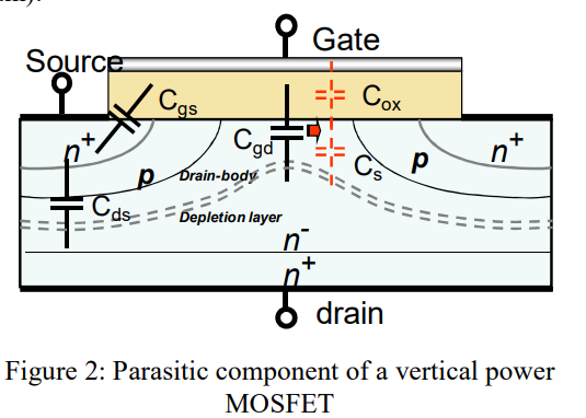
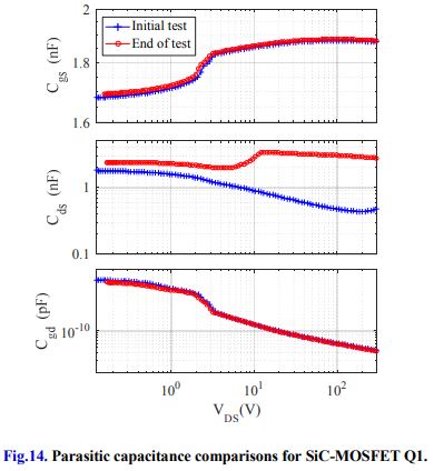
Please take a look at the following images, experimentally obtained from a power cycling test of a power MOSFET. After the test where thermal aging is created due to repetitive power cycles, it is found that the parasitic capacitance Cds (drain-to-source) is significantly influenced, but the two parasitic capacitances Cgd (gate-to-drain) and Cgs (gate-to-source) are not significantly affected by the test. What is the reason behind that?
2 Answers
That is not a cross-section of a power (high voltage) MOSFET. Such a device has an 'extended drain' region where depletion regions gros as drain V is increased and shield the gate oxide at the drain end from the high votlages -- else the deice would breakdown.
Without knowing the stress conditions, it is not possible to explain the change in CDS (especially when there are not corresponding changes in other parameters), but it appears to be some type of breakdown or creepage path in the device. You need to show the DC charactersistics to get a better insight.
There exists an Infineon application note, Repetitive Avalanche of Automotive MOSFETs that talks about the drift of output capacitance, \$C_{OSS} = C_{GD}+C_{DS}\$ (page 11, Section 6, Failure modes – repetitive avalanche):
... the failure mechanisms in repetitive avalanche can be categorized in two failure modes:
- degradation of materials in particular the top side metallization due to the high number of temperature cycles leading eventually to a drift in device parameters such as the on-state resistance,
- drift of device parameters such as the leakage currents, the drain to source voltage or output capacitance due to high electrical stress during the avalanche event possibly caused by hot carrier injection.
Repetitive avalanche is one of several phenomena accompanying your "repetitive power cycles", if I am correct in guessing that you used the statistical approach when testing the devices for failures. Repetitive avalanche may happen during regular operation and usually does not result in a catastrophic failure. It causes only unavoidable aging.
The drain voltage range for \$C_{OSS}\$ measurements is not specified in the application note, but, as we learn about repetitive avalanche from Infineon's documents Application Note AN-1005 and Some key facts about avalanche, the most likely location for the onset of avalanche breakdown is the drain side of the channel, the region that affects the \$C_{DS}\$ vs. \$V_{DS}\$ graph in the saturation mode, i.e., at higher \$V_{DS}\$ values. I discussed this phenomenon answering the question Why does the breakdown always occur on the drain side for MOSFET?
Summing up, the \$C_{DS}\$ drift you measured is a possible result of hot carrier degradation. Hot carriers accumulate in the channel in the vicinity of the drain, and, in the framework of the hot carrier degradation hypothesis, the phenomenon would not manifest itself in your \$C_{GS}, \, C_{GD}\$ graphs.


