0
\$\begingroup\$

I built the following pulse-width-recognition/digital-filter circuit on a solderless breadboard. I used 1/4 of a CD4011BE with another 1 µF bypass capacitor as the inverter, a perfboarded CD4060 circuit that has been verified to work as the 512 Hz clock source (CLK), and my AFG-2012 as the 2.5 Hz/90% duty input signal source (SIG):
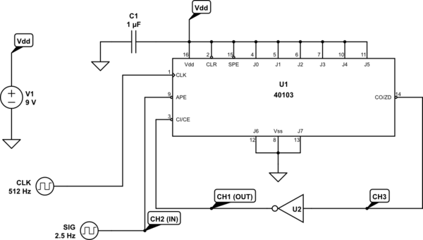
schematic

simulate this circuit – Schematic created using CircuitLab

Instead of getting a "clean" output from the circuit of any sort, I get erratic output from the counter instead (channel numbers are as shown in the schematic, ignore the labels I have set on the scope):

scope screenshot of faulty output waveform (only comes up to Vcc/2, with HF oscillations on top)

Is this a sign that I accidentally fried my counter chip and should replace it (with better attention to ESD precautions and so on), or is my concept of operations, namely that the counter "freezes" itself at 0 after counting down until the input signal goes low again, hopeless to begin with?

Update: I tried putting a new counter chip on my breadboard, taking proper ESD precautions in the process, and the circuit's behavior did not change. Can someone explain to me why the circuit I have is behaving the way it is?

Update 2: with the replacement counter chip installed, I tried taking a pair of new scope shots, one of the overall behavior and one zoomed in on the rising edge of the output, both with the clock as CH3 instead of the original use of it to directly monitor the counter's output.

scope shot of faulty waveform with clock shown

scope shot zoomed in on initial rising edge of faulty output waveform

Update again: was able to get a full-sample-rate zoomed in shot (and fixed the coupling issue on CH3):

zoomed in shot with a better view of the oscillations

Another update: I got a shot at 250MSa/s + 6MPts with the timebase at 50ns/div when the capture was taken, using an inter-channel delay trigger to set the trigger edge where I wanted it:

yet another scope shot showing hopefully more details

\$\endgroup\$
13
  • \$\begingroup\$ The scope traces are a mess. Reduce the gain on each channel to eg. 5V/div, and separate them vertically so they don't run into each other. Switch CH3 from AC to DC. Zoom in on area where CH3 is going up and down, and put the clock input on CH4 to verify that the signal is good and to compare the timing. \$\endgroup\$ Commented Oct 15, 2022 at 5:41
  • \$\begingroup\$ @BruceAbbott -- I switched CH3 from the output node it was on to the clock node, given that I know the NAND-inverter is functional, and my clock is indeed fine (a nice 510Hz squarewave). I can get you two shots, one zoomed out and the other zoomed in... \$\endgroup\$ Commented Oct 15, 2022 at 15:35
  • \$\begingroup\$ @BruceAbbott -- posted an update with the new screenshots \$\endgroup\$ Commented Oct 15, 2022 at 17:51
  • 1
    \$\begingroup\$ Waveforms look good now. I will analyze it when I have time... \$\endgroup\$ Commented Oct 16, 2022 at 21:02
  • 1
    \$\begingroup\$ @ThreePhaseEel No, it's how quantized it looks. That could be more bit depth than sample count though, come to think of it. \$\endgroup\$
    – Hearth
    Commented Oct 16, 2022 at 21:25

1 Answer 1

1
\$\begingroup\$

What appears to be happening is the CD40103 counts down from 255 to 0 (which takes ~40 ms) causing CO/ZD to go low ~90 ns after the clock rising edge, as expected. However this is then fed through the inverter to CI/CE, causing it to go high ~30 ns later which then makes CI/CE go low again. This cycle repeats a random number of times until the counter resets and counts down from 255 again.

The operation of control inputs to the CD40103 is quite complex, and the timing diagram only shows a few of the possible combinations. According to the datasheet counting is inhibited when CI/CE is high. However if all inputs except CI/CE are high at the time of zero count (CO/ZD low), the counter is reset to maximum count and counting is enabled.

I suspect that disabling and then re-enabling CI/CE so soon after clocking causes a race condition where the counter doesn't get properly reset and just toggles CO/ZD and CI/CE alternately for while, until eventually it does reset and counts down normally.

I'm not sure what you are trying to do with this circuit. If you want the count to stop at zero until SIG goes low then perhaps what you need is a bistable latch that is set by CO/ZD going low and reset by SIG going low. This can be made with 2 NAND gates in place of the inverter. You may still have trouble if SIG changes state at the same time as CLK, in which case you could feed SIG through a D flip-flop to synchronize it.

\$\endgroup\$
1
  • \$\begingroup\$ Yeah, I took another look at the logic diagram in datasheet and found the gating line that is doing that (I missed it earlier -- it's not exactly in the place one'd expect to find it, for sure). I'll probably wind up going with the latch approach, although I may need to go with a NOR instead of a NAND latch in order to get it to be reset dominant (vs set dominant) \$\endgroup\$ Commented Oct 17, 2022 at 22:19

Your Answer

By clicking “Post Your Answer”, you agree to our terms of service and acknowledge you have read our privacy policy.

Not the answer you're looking for? Browse other questions tagged or ask your own question.