0
\$\begingroup\$

I am new to high speed design .Please don't flame me if this question is very basic :)

Below statement is from AD application note. (AD Appnote)

"The ground plane not only acts as a low impedance return path for decoupling high-frequency currents (caused by fast digital logic) but also minimizes EMI/RFI emissions. Because of the shielding action of the ground plane, the circuit’s susceptibility to external EMI/RFI is also reduced."

But it does not explain how these things happening. I have 2 questions.

  1. May I know how ground plane acts as a low impedance return path.

  2. Can someone explain Shelding action of GND plane.

\$\endgroup\$
5
  • 2
    \$\begingroup\$ The ground return currents will flow back to source directly underneath the signal trace. This happens because that becomes the path of least-resistance (or more correctly, path of least impedance). It has to do with loop area... The area of the loop following the path directly under the trace is at a minimum. Any other path is a bigger loop, hence higher impedance. See Faradays law. Suggest you buy a real book on the topic rather than trying piece together a picture in your head from app notes. "High Speed Digital Design - a Handbook of Black Magic" is one of the more popular options. \$\endgroup\$
    – Kyle B
    Commented Oct 21, 2022 at 5:30
  • \$\begingroup\$ @ Kyle,Thank you very much. definitely I will buy that book. Lower the loop area lower the impedance. Please correct me if I am wrong. \$\endgroup\$
    – Confused
    Commented Oct 21, 2022 at 5:35
  • 2
    \$\begingroup\$ @Hari The book also has errors. And, after all, it is 1993! But it is a good book to get, regardless. Go here for some of the errata circa 2011. \$\endgroup\$
    – jonk
    Commented Oct 21, 2022 at 5:41
  • \$\begingroup\$ @ Jonak,Thank you.can you please explain the shielding effect of Ground plane \$\endgroup\$
    – Confused
    Commented Oct 21, 2022 at 5:49
  • 1
    \$\begingroup\$ Question yourself for what you are shielding. A ground-/returnplane is not like a magical carpet, which makes everything neutral. Shielding is done for E-fields and H-fields. \$\endgroup\$
    – RemyHx
    Commented Oct 21, 2022 at 10:11

2 Answers 2

4
\$\begingroup\$

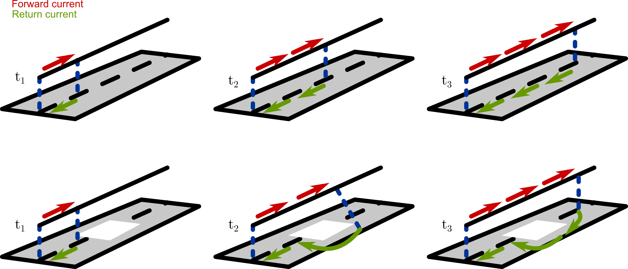
Return current is an important concept in any high speed design. The concept is illustrated in this figure:

enter image description here

The first row of images show what happens with a proper return current. The ground plane acts as a conductor for the return current that is caused by the change in electric field as the pulse propagates through the wire.

In the second row of images, an opening is made underneath the wire. This does not mean that there is no return current, but it simply means that the return current must make a detour around the hole in the ground plane.

If the return current is further away from the forward current, then the loop becomes larger. The problem with this is that a larger loop provides a better coupling to other (nearby) loops through Maxwell's law of induction and Ampère's circuital law, or in other words: electromagnetic interference.

\$\endgroup\$
2
\$\begingroup\$

Can someone explain Shelding action of GND plane.
Any conductor will block electric fields from permiating though it. Shields can be made from conductors (a Faraday cage is a box made from conductors, the potential inside will be zero). So the ground plane(s) in a PCB can block electric fields and also redirect currents back to the source.

May I know how ground plane acts as a low impedance return path.

In short two conductors form a capacitor, this also applies to ground planes. The trace above and the plane below form a capacitor (usually very small, 1sq inch on a PCB between ground and another plane will be in the pf range, traces smaller than that), changing currents (high frequency) can flow though the FR4 and return to ground where they can be returned to the source.

\$\endgroup\$
1
  • \$\begingroup\$ I thought that the inductance effects were more significant than the capacitance effects here. A single trace is an inductor (high impedance); a trace and a ground plane form a common-mode choke instead (low impedance to equal currents in opposite directions). \$\endgroup\$ Commented Oct 24, 2022 at 11:43

Your Answer

By clicking “Post Your Answer”, you agree to our terms of service and acknowledge you have read our privacy policy.

Not the answer you're looking for? Browse other questions tagged or ask your own question.